Flash (Hardware): Difference between revisions
Jump to navigation
Jump to search
m (→Flash) |
|||
| (48 intermediate revisions by 3 users not shown) | |||
| Line 1: | Line 1: | ||
= Flash = | = Flash = | ||
The PS3 uses a NOR interface from the [[South Bridge]] to address the main firmware flash. On NAND based consoles, it uses the [[Starship2]] as an interleaving bridge chip to the two NAND flash, while on NOR based consoles the single NOR flash is connected directly to the [[South Bridge]]. | The PS3 uses a NOR interface from the [[South Bridge]] to address the main firmware flash. On NAND based consoles, it uses the [[Starship2]] as an interleaving bridge chip to the two NAND flash, while on NOR based consoles the single NOR flash is connected directly to the [[South Bridge]]. | ||
<Gallery> | |||
File:Spansion flash product code.jpg|Spansion flash<br>product code | |||
</Gallery> | |||
== SKU Differentiation == | == SKU Differentiation == | ||
For a difference between models, see [[SKU Models]] | For a difference between models, see [[SKU Models]] | ||
===Retail=== | |||
{{Flash types and models used by PS3}} | |||
{ | |||
{ | |||
===Non Retail=== | |||
Reference Tool DECR1000A Communication Processor board : | |||
1x [[K9F2G08U0M|Samsung K9F2G08U0M]] (NAND 1x2Gbit=256MB total) | |||
== Other Flash == | |||
=== Renesas HN58X2504TIE (EEPROM) === | |||
<div style="float:right">[[File:TSSOP-8pin-HN58X2504TIE.png|200px|thumb|left|8-pin TSSOP<br />Renesas HN58X2504TIE]]</div> | <div style="float:right">[[File:TSSOP-8pin-HN58X2504TIE.png|200px|thumb|left|8-pin TSSOP<br />Renesas HN58X2504TIE]]</div> | ||
Note: although [http://www.edepot.com/playstation3.html#Super_Secrets edepot&others] lists it on the board, I can only find this IC in the sixaxis. <br /> | Note: although [http://www.edepot.com/playstation3.html#Super_Secrets edepot&others] lists it on the board, I can only find this IC in the sixaxis. <br /> | ||
| Line 666: | Line 71: | ||
|- | |- | ||
|} | |} | ||
{{Motherboard Components}}<noinclude>[[Category:Main]]</noinclude> | |||
Latest revision as of 18:46, 30 October 2015
Flash[edit | edit source]
The PS3 uses a NOR interface from the South Bridge to address the main firmware flash. On NAND based consoles, it uses the Starship2 as an interleaving bridge chip to the two NAND flash, while on NOR based consoles the single NOR flash is connected directly to the South Bridge.
Spansion flash
product code

SKU Differentiation[edit | edit source]
For a difference between models, see SKU Models
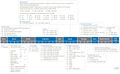
Retail[edit | edit source]
| Flash Type / Model | PS3 Fat | PS3 Slim | PS3 SuperSlim | notes | |||||||||||||||||
|---|---|---|---|---|---|---|---|---|---|---|---|---|---|---|---|---|---|---|---|---|---|
| CECHA CECHB |
CECHC CECHE |
CECHE | CECHG | CECHH | CECHJ CECHK |
CECHL CECHM CECHP CECHQ |
CECH-20xx | CECH-21xx | CECH-25xx | CECH-25xx | CECH-30xx | CECH-40xx | CECH-40xx | CECH-40xx '12GB' noHDD | |||||||
| COK 001 |
COK 002 |
COK 002W |
SEM 001 |
DIA 001 |
DIA 002 |
VER 001 |
DYN 001 |
SUR 001 |
JTP 001 |
JSD 001 |
KTE 001 |
MSX 001 |
MPX 001 |
MPX 001 | |||||||
| NAND | 2x Samsung K9F1G08U0A-PIB0 | Yes | Yes | Yes | - | No | No | No | No | No | No | No | No | No | No | No | |||||
| 2x Samsung K9F1G08U0B-PIB0 | - | - | - | Yes | No | No | No | No | No | No | No | No | No | No | No | ||||||
| NOR | 1x Spansion S29GL128N90TFIR2 | No | No | No | No | Yes | Yes | Yes | Yes | - | - | - | - | - | - | No | |||||
| 1x Samsung K8Q2815UQB-PI4B | No | No | No | No | - | - | Yes | Yes | Yes | - | - | - | - | - | No | ||||||
| 1x Spansion S29GL128P90TFIR2 | No | No | No | No | - | - | Yes | Yes | Yes | Yes | Yes | Yes | Yes | Yes | No | ||||||
| 1x Macronix MX29GL128ELT2I-90G | No | No | No | No | - | - | - | Yes | Yes | Yes | yes ? | Yes | No | ||||||||
| 1x Samsung K8P2716UZC-QI4D | No | No | No | No | Yes | - | - | - | - | Yes | Yes | Yes | No | ||||||||
| 1x Macronix MX29GL128FLT2I-90G | No | No | No | No | - | - | - | - | - | - | - | - | Yes | Yes | No | ||||||
| eMMC | 1x Panasonic MN66840 + 1x Samsung KLMAG2GE4A-A001 |
No | No | No | No | No | No | No | No | No | No | No | No | No | No | Yes | |||||
| connection type | NAND layout 1 | NOR layout 1 | NOR layout 2 | NOR layout 3 | NOR layout 4 | NOR layout 5 | eMMC layout | ||||||||||||||
Non Retail[edit | edit source]
Reference Tool DECR1000A Communication Processor board : 1x Samsung K9F2G08U0M (NAND 1x2Gbit=256MB total)
Other Flash[edit | edit source]
Renesas HN58X2504TIE (EEPROM)[edit | edit source]

Note: although edepot&others lists it on the board, I can only find this IC in the sixaxis.
Datasheet
productcode meaning:
H -
N -
5 -
8 - Organisation : x8bit
X -
2 -
5 -
0 -
4 - Density : 4-kbit (512x8bit)
T - Package : 8pin plastic TSSOP (TTP-8DAV)
I - Temp : Industrial (-40 to +85 °C
E - Environment : Lead Free
Each PS3 has a special EEPROM chip on the motherboard using a SPI Serial Interface Renasas chip.
| Type | Size | Speed | Voltage | Packaging | Manufacturer | Serial Number | Description |
|---|---|---|---|---|---|---|---|
| EEPROM | 4-kbit (512x8bit) | 3MHz | 1.8V to 5.5V | 8-pin TSSOP | Renesas | HN58X2504TIE | PS3 EEPROM chip |
| Pin | Usage | Remarks |
|---|---|---|
| 1 | S | Chip Select |
| 2 | Q | Serial data output |
| 3 | W | Write Protect |
| 4 | VSS | Ground |
| 5 | D | Serial data input |
| 6 | C | Serial Clock |
| 7 | HOLD | Hold |
| 8 | VCC | Vcc (min 1.8V-max 5.5V) |
| |||||||||||||||||||||||||||||||||||||||||||||||||||||||||||||||||||||||||||||||||||||||||||||||||||||||||||||||||||||||||||||||||||||||||||||||||||||||||||||||||||||||||||||
