RSX
RSX - Reality Synthesizer
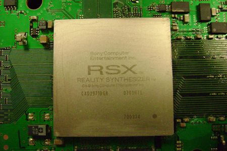
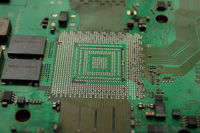
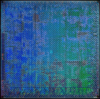
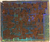
The RSX 'Reality Synthesizer' is a proprietary graphics processing unit (GPU) codeveloped by Nvidia and Sony for the PlayStation 3 game console. It is a GPU based on the Nvidia 7800GTX graphics processor and, according to Nvidia, is a G70/G71 (previously known as NV47) hybrid architecture with some modifications. The RSX has separate vertex and pixel shader pipelines. The GPU makes use of 256 MB GDDR3 RAM clocked at 650 MHz with an effective transmission rate of 1.4 GHz and up to 224 MB of the 3.2 GHz XDR main memory via the CPU (480 MB max).
Specifications
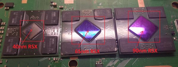
- 500 MHz on 90 nm process (shrunk to 65 nm in 2008 and to 40 nm in 2010)
- Based on NV47 Chip (Nvidia GeForce 7800 Architecture)
- early development tools had NV47 with 256 bit local memory interface and 16 ROPs
- later RSX with 128bit local memory interface and 8 ROPs
- Little Endian
- 300+ million transistors
- Multi-way programmable parallel floating-point shader pipelines
- Independent pixel/vertex shader architecture
- 24 parallel pixel-shader ALU pipes clocked @ 550 MHz
- 5 ALU operations per pipeline, per cycle (2 vector4 , 2 scalar/dual/co-issue and fog ALU, 1 Texture ALU)
- 27 floating-point operations per pipeline, per cycle
- 8 parallel vertex pipelines
- 2 ALU operations per pipeline, per cycle (1 vector4 and 1 scalar, dual issue)
- 10 FLOPS per pipeline, per cycle
- Floating Point Operations: 400.4 Gigaflops ((24 * 27 Flops + 8 * 10 Flops) * 550)
- 24 texture filtering units (TF) and 8 vertex texture addressing units (TA)
- 24 filtered samples per clock
- Maximum Texel fillrate: 12.0 GigaTexels per second (24 textures * 500 MHz)
- 32 unfiltered texture samples per clock, ( 8 TA x 4 texture samples )
- 24 filtered samples per clock
- 8 Render Output units / pixel rendering pipelines
- Peak pixel fillrate (theoretical): 4.0 Gigapixel per second
- Maximum Z-buffering sample rate: 8.0 GigaSamples per second (2 Z-samples * 8 ROPs * 500 MHz)
- Maximum Dot product operations: 51 billion per second (combined with Cell CPU)
- 128-bit pixel precision offers rendering of scenes with High dynamic range rendering
- 256 MB GDDR3 RAM at 650 MHz
- Earlier PS3 Models: Samsung K4J52324QC-SC14 rated max 700MHz
- Later PS3 Models: Qimonda HYB18H512322AF-14 (seen on CXD2971DGB)
- 128-bit memory bus width
- 22.4 GB/s read and write bandwidth
- Cell FlexIO bus interface
- Rambus XDR Memory interface bus width: 56bit out of 64bit (serial)
- 20 GB/s read to the Cell and XDR memory
- 15 GB/s write to the Cell and XDR memory
- Support for PSGL (OpenGL ES 1.1 + Nvidia Cg)
- Support for S3 Texture Compression
More features are revealed in the following chart delineating the differences between the RSX and the nVidia 7800 GTX.
| Difference | RSX | nVidia 7800GTX |
|---|---|---|
| GDDR3 Memory bus | 128bit | 256bit |
| ROPs | 8 | 16 |
| Post Transform and Lighting Cache | 63 max vertices | 45 max vertices |
| Total Texture Cache Per Quad of Pixel Pipes (L1 and L2) | 96kB | 48kB |
| CPU interface | FlexIO | PCI-Express 16x |
| Technology | 28nm/40nm/65nm/90nm | 110nm |
Other RSX features/differences include:
   More shader instructions
       Extra texture lookup logic (helps RSX transport data from XDR)
       Fast vector normalize
Note that the cache (Post Transform and Lighting Vertext Cache) is located between the vector shader and the triangle setup.
A sample flow of data inside the RSX would see them first processed by 8 vertex shaders. The output are then sent to the 24 active pixel shaders, which can involve the 24 active texture units. Finally, the data is passed to the 8 Raster Operation Pipeline units (ROPs), and on out to the GDDR3. Note that the pixel shaders are grouped into groups of four (called Quads). There are 7 Quads, with 1 redundant, leaving 6 Quads active, which provides us with the 24 active pixel shaders listed above (6 times 4 equals 24). Since each Quad has 96kB of L1 and L2 cache, the total RSX texture cache is 576kB. General RSX features include 2x and 4x hardware anti-aliasing, and support for Shader Model 3.0.
Serial Numbers @ SKU's
| PS3 Model | Mobo Model | Mobo serial | RSX Serial | Die Tech | Die Size | Remark |
|---|---|---|---|---|---|---|
| CECHAxx | COK-001 | 1-871-868-12 | CXD2971GB | 90nm | 258mm² | edepot ps3secrets |
| CECHAxx | COK-001 | 1-871-868-12 | CXD2971AGB | 90nm | 258mm² | |
| CECHAxx | COK-001 | 1-871-868-22 | CXD2971DGB | 90nm | 258mm² | |
| CECHAxx | COK-001 | 1-871-868-32 | CXD2971DGB | 90nm | 258mm² | |
| CECHAxx | COK-001 | 1-871-868-32 | CXD2971AGB | 90nm | 258mm² | |
| CECHBxx | COK-001 | 1-871-868-22 | CXD2971DGB | 90nm | 258mm² | edepot ps3secrets |
| CECHBxx | COK-001 | 1-871-868-32 | CXD2971DGB | 90nm | 258mm² | edepot ps3secrets |
| CECHCxx | COK-002 | 1-873-513-11 | CXD2971DGB | 90nm | 258mm² | edepot ps3secrets |
| CECHCxx | COK-002 | 1-873-513-21 | CXD2971GB | 90nm | 258mm² | |
| CECHCxx | COK-002 | 1-873-513-31 | CXD2971DGB | 90nm | 258mm² | |
| CECHExx | COK-002W | 1-873-513-xx | -? | 90nm | 258mm² | |
| CECHGxx | SEM-001 | 1-875-384-xx | CXD2971DGB | 90nm | 258mm² | |
| CECHGxx | SEM-001 | 1-875-384-xx | CXD2971BGB or: CXD2971DGB |
90nm | 258mm² | |
| CECHGxx | SEM-001 | 1-875-384-xx | CXD2971AGB | 90nm | 258mm² | |
| CECHGxx | SEM-001 | 1-875-384-xx | CXD2971DGB | 90nm | 258mm² | edepot ps3secrets |
| CECHHxx | DIA-001 | 1-875-938-11 | CXD2971AGB | 90nm | 258mm² | |
| CECHHxx | DIA-001 | 1-875-938-31 | CXD2971-1GB | 90nm | 258mm² | |
| CECHHxx | DIA-001 | 1-875-368-11 | CXD2971-1GB | 90nm | 258mm² | |
| CECHHxx | DIA-001 | 1-875-368-11 | CXD2971AGB | 90nm | 258mm² | |
| CECHHxx | DIA-001 | 1-875-368-11 | CXD2971AGB | 90nm | 258mm² | edepot ps3secrets |
| CECHJxx | DIA-002 | 1-876-912-xx | CXD2982GB | 65nm | ? 186mm² ? | |
| CECHKxx | DIA-002 | 1-876-912-32 | CXD2982BGB | 65nm | ? 186mm² ? | |
| CECHKxx | DIA-002 | 1-876-912-42 | CXD2982GB | 65nm | ? 186mm² ? | |
| CECHKxx | DIA-002 | 1-876-912-xx | CXD2982GB | 65nm | ? 186mm² ? | edepot ps3secrets |
| CECHLxx | VER-001 | 1-878-196-31 | CXD2991GB | 65nm | ? 186mm² ? | |
| CECHLxx | VER-001 | 1-878-196-31 | CXD2991GB | 65nm | ? 186mm² ? | edepot ps3secrets |
| CECHMxx | VER-001 | 1-878-196-31 | -? | 65nm | ? 186mm² ? | |
| CECHPxx | VER-001 | 1-878-196-31 | -? | 65nm | ? 186mm² ? | |
| CECHQxx | VER-001 | 1-878-196-31 | -? | 65nm | ? 186mm² ? | |
| CECH-20xx | DYN-001 | 1-880-055-31 | CXD2991CGB | 65nm | ? 186mm² ? | |
| CECH-20xx | DYN-001 | 1-880-055-31 | CXD2991EGB | 65nm | ? 186mm² ? | |
| CECH-20xx | DYN-001 | 1-880-055-31 | CXD2991EGB | 65nm | ? 186mm² ? | edepot ps3secrets |
| CECH-20xx | DYN-001 | 1-880-055-31 | CXD2991GGB | 65nm | ? 186mm² ? | |
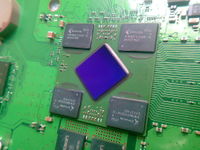
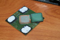
| CECH-21xx | SUR-001 | 1-881-945-11 | CXD5300AGB | 40nm (with IHS, 4 VRAM chips) | ? 114mm² ? | |
| CECH-21xx | SUR-001 | 1-881-945-11 | CXD5300AGB | 40nm (with IHS, 4 VRAM chips) | ? 114mm² ? | edepot ps3secrets |
| CECH-25xx | JTP-001 | 1-882-481-11 | CXD5300A1GB | 40nm (with IHS, 4 VRAM chips) | ? 114mm² ? | edepot ps3secrets |
| CECH-25xx | JTP-001 | 1-882-481-21 | CXD5300A1GB | 40nm (with IHS, 4 VRAM chips) | ? 114mm² ? | |
| CECH-25xx | JSD-001 | 1-882-770-11 | CXD5300A1GB | 40nm (with IHS, 4 VRAM chips) | ? 114mm² ? | edepot ps3secrets |
| CECH-25xx | JSD-001 | 1-882-770-31 | CXD5300CGB | 40nm (with IHS, 4 VRAM chips) | ? 114mm² ? | |
| CECH-30xx | KTE-001 | 1-884-749-11 | CXD5301DGB | 40nm (with IHS, 4 VRAM chips) | ? 114mm² ? | |
| CECH-30xx | KTE-001 | 1-884-749-31 | CXD5301A1GB | 40nm (with IHS, 4 VRAM chips) | ? 114mm² ? | |
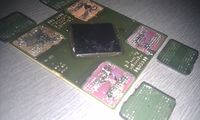
| CECH-40xx | MSX-001 | 1-886-928-11 | CXD5302DGB | 40nm (without IHS, 4 VRAM chips) | ? 114mm² ? | |
| CECH-40xx | MPX-001 | 1-887-233-11 | CXD5302A1GB | 40nm (without IHS, 4 VRAM chips) | ? 114mm² ? | pocketnews dissasembly |
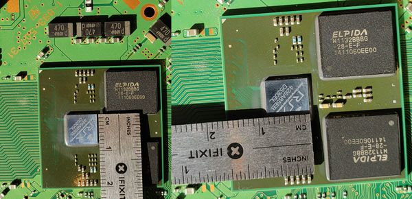
| ? | NPX-001 | ? | ? | 28nm (without IHS, 2 VRAM chips) | ? 68mm² ? | |
| CECH-40xx | PQX-001 | 1-888-629-22 | D5305K | 28nm (without IHS, 2 VRAM chips) | ? 68mm² ? | mobile01_tw |
| ? | PPX-001 | ? | ? | 28nm (without IHS, 2 VRAM chips) | ? 68mm² ? | |
| CECH-43xx | RTX-001 | ? | ? | 28nm (without IHS, 2 VRAM chips) | ? 68mm² ? | |
| CECH-43xx | REX-001 | 1-893-507-31 | D5305L | 28nm (without IHS, 2 VRAM chips) | ? 68mm² ? |
Alternative list
- CXD2971xxx (RSX 90nm, with IHS, 4 VRAM chips)
- CXD2982xxx (RSX 65nm, with IHS, 4 VRAM chips)
- Motherboards: DIA-002
- CXD2991xxx (RSX 65nm, with IHS, 4 VRAM chips)
- CXD5300xxx (RSX 40nm, with IHS, 4 VRAM chips)
- CXD5301xxx (RSX 40nm, with IHS, 4 VRAM chips)
- Motherboards: KTE-001
- CXD5302xxx (RSX 40nm, without IHS, 4 VRAM chips)
- D5305x (RSX 28nm, without IHS, 2 VRAM chips)
Local GDDR3 Memory Physical Structure
- Total Memory 256MB
- 2 Partitions (128MB)
- 64bit bus per partition
- 8 Banks per partition (16MB)
- 4096 Pages per bank (4KB) -> 12bit Row Address
- Memory block in a page -> 9bit Column Address
- Minimum access granularity = 8 bytes -> same as buswidth between RSX <> GDDR
Software
RSX Memorymap
Although the RSX has 256MB of GDDR3 RAM, not all of it is useable. The last 4MB is reserved for keeping track of the RSX internal state and issued commands. The 4MB of GPU Data contains RAMIN, RAMHT, RAMFC, DMA Objects, Graphic Objects, and the Graphic Context. The following is a breakdown of the address within 256MB of the RSX.
| Address Range | Size | Comment |
|---|---|---|
| 0000000-FBFFFFF | 252 MB | Framebuffer |
| FC00000-FFFFFFF | 4 MB | GPU Data |
| FF80000-FFFFFFF | 512KB | RAMIN: Instance Memory |
| FF90000-FF93FFF | 16KB | RAMHT: Hash Table |
| FFA0000-FFA0FFF | 4KB | RAMFC: FIFO Context |
| FFC0000-FFCFFFF | 64KB | DMA Objects |
| FFD0000-FFDFFFF | 64KB | Graphic Objects |
| FFE0000-FFFFFFF | 128KB | GRAPH: Graphic Context |
Besides local GDDR3 memory, main XDR memory can be accessed by RSX too, which is limited to either:
- 0MB - 256MB (0x00000000 - 0x0FFFFFFF)
- -or-
- 0MB - 512MB (0x00000000 - 0x1FFFFFFF)
Speed, Bandwidth, and Latency
System bandwith (theoretical maximum):
- Cell to/from 256MB XDR : 25.6 GB/s
- Cell to RSX (IOIFO): 20GB/s (practical : 15.8GB/s @ packetsize 128B)
- Cell from RSX (IOIFI) : 15GB/s (practical : 11.9GB/s @ packetsize 128B)
- RSX to/from 256MB GDDR3 : 20.8GB/s (@ 650MHz)
Because of the aforementioned layout of the communication path between the different chips, and the latency and bandwidth differences between the various components, there are different access speeds depending on the direction of the access in relation to the source and destination. The following is a chart showing the speed of reads and writes to the GDDR3 and XDR memory from the viewpoint of the Cell and RSX. Note that these are measured speeds (rather than calculated speeds) and they should be worse if RSX and GDDR3 access are involved because these figures were measured when the RSX was clocked at 550Mhz and the GDDR3 memory was clocked at 700Mhz. The shipped PS3 has the RSX clocked in at 500Mhz (front and back end, although the pixel shaders run separately inside at 550Mhz). In addition, the GDDR3 memory was also clocked lower at 650Mhz.
speed table
| Processor | 256MB XDR | 256MB GDDR3 |
|---|---|---|
| Cell Read | 16.8GB/s | 16MB/s (15.6MB/s @ 650MHz) |
| Cell Write | 24.9GB/s | 4GB/s |
| RSX Read | 15.5GB/s | 22.4GB/s (20.8GB/s @ 650MHz) |
| RSX Write | 10.6GB/s | 22.4GB/s (20.8GB/s @ 650MHz) |
Because of the VERY slow Cell Read speed from the 256MB GDDR3 memory, it is more efficient for the Cell to work in XDR and then have the RSX pull data from XDR and write to GDDR3 for output to the HDMI display. This is why extra texture lookup instructions were included in the RSX to allow loading data from XDR memory (as opposed to the local GDDR3 memory).
ROM Versions
These are the listed RSX ROM (aka Vbios) versions info we have collected from lv1 debug ouput
DEH/DECR-1000:
[INFO]: BE:3.1, SB:DX3.1
rsx:      a01 420/600 vpe:ff shd:3f [AE0000915:0:1:16:b:f:1:1:1]

[INFO]: BE:3.1, SB:DX3.1
rsx:      a02 420/600 vpe:ff shd:3f [F9A458700:0:2:3:b:f:3:1:1][0:0:0:0:0:3]

[INFO]: BE:3.1, SB:DX3.2
rsx:      b01 500/650 vpe:ff shd:3f  [G1A834800:1:2:2:3:6:3:9:1][16:3:0:0:1:2:1][0:0:0]

[INFO]: BE:3.1, SB:DX3.2
rsx:      b01 500/650 vpe:ff shd:5f [AE0000993:0:1:13:c:a:1:4:2][16:3:0:0:1:3:0]

[INFO]: BE:3.1, SB:DX3.2
rsx:      b01 500/600 vpe:ff shd:77 [FCA684200:0:2:2:f:7:3:5:1][0:0:0:0:0]

[INFO]: BE:3.1, SB:DX3.2
rsx:      b01 500/650 vpe:ff shd:7d [G1A778601:1:2:15:7:10:3:7:2][16:3:0:0:1:3:0]

[INFO]: BE:3.1, SB:DX3.2
rsx:      b02 500/650 vpe:ff shd:3f  [G2A874100:1:2:e:4:6:3:9:2][16:3:0:0:1:2:1][0:0:0]

[INFO]: BE:3.1, SB:DX3.2
rsx:      b03 500/650 vpe:ff shd:7b  [GAB886100:1:2:17:f:5:3:f:2][16:3:0:0:1:3:1][0:0:0]

[INFO]: BE:3.1, SB:DX3.2
rsx: b03 500/650 vpe:ff shd:7b [GAB886100:1:2:4:7:5:3:f:2][16:3:0:0:1:3:1][0:0:0]

[INFO]: BE:3.1, SB:DX3.2
rsx: b07 500/650 vpe:ff shd:3f [J3E106900:1:2:c:b:6:3:12:1][16:3:2:0:1:3:1][0:0:0]

[INFO]: BE:3.1, SB:DX3.2
rsx:      b07 500/650 vpe:ff shd:3f  [J3E107200:1:2:a:6:3:3:12:1][16:3:2:0:1:3:1][0:0:0]

[INFO]: BE:3.1, SB:DX3.2
rsx:      b07 500/650 vpe:ff shd:3f  [J3E078500:1:2:11:c:f:3:12:1][16:3:2:0:1:3:1][0:0:0]
DECR-1400:
rsx: rsx65 a06 500/650 vpe:ff shd:6f [AP0013056:1:1:f:13:11:2:5:2][1c:0:2:0:1:2:0][2:1:0]
DECHA00A (January 2007):
rsx: b08 500/650 vpe:ff shd:3f [AP0008286:1:1:14:e:b:2:11:1][39:2:1:1:1:3:1][0:0:0]
DECH2000A (September 2009):
rsx: rsx65 a06 500/650 vpe:ff shd:6f [AP0015079:1:1:b:14:14:2:5:2][1c:0:2:0:1:2:0][2:1:0]
RETAIL:
[INFO]: BE:3.1, SB:DX3.1
rsx:      b08 1f4/28a vpe:ff shd:3f  [AP0004687:1:1:14:13:a:2:f:1][16:3:1:1:1:3:1][0:0:0]

CECH-2500
rsx:      rsx40 a01 500/650 vpe:ff shd:3f  [NN3108-17:0:4:11:c:3:6:0:1][28:0:a:0:1:0:1][1:1:0]

CECH-30xx
[INFO]: BE:12S DD2.0, SB:ZX1.2
rsx:      rsx40 a01 500/650 vpe:ff shd:3f  [N3T552-09:0:4:9:13:14:6:0:1][22:0:a:0:1:0:1][1:1:0]
Speculatively it is likely that the very first numbers are the actual rom version (a01, b01, b03, b07, b08...) despite Sony's documentation claiming otherwise, DECR-1000 units with rom version b07 and above (and perhaps some others that have not yet been encountered) are not capable of running any firmware lower than 1.60 (from sdk 160.008) this is because the rom version is unknown/unsupported in older lv1 which will fail to initialize the RSX hardware and will cause lv1 to output a "rsx rom abort!" message, this will in turn create an exception early in lv2 boot process as it tries to use the RSX and creates a hard brick several RSX related errors such as "lv2(2): # __rsxaudio_intr_create_thread 983 ffffffff" or "graphics error 512 : 00012625 c221bbb0" ; "lv2(2): page fault handler (DSI): invalid access address 0x795d00e8!".
There is nothing in the documentation warning you about this and there is nothing preventing you (or a legitimate developer) to install an unsupported firmware as the vsh allows updating/downgrading to 1.00 or higher and the min praxis for those units is actually lower than 1.00. (0.08 to be exact) Should this issue occur to you, other than sending the unit back to Sony for servicing, the only way to fix this is to flash an ebootrom (as lv0 still runs fine and is in charge of handling flashing the system memory through lcnslsrv) the problem with that is that sony never released/issued an ebootrom for a firmware higher than 1.00.002 , so officially one would have no choice but to return the unit, that said, considering the ebootrom format is not rocket science and is actually documented (it's a very slight variation of the coreos package format, there are no specific checks whatsoever preventing you from crafting your own, it is not hashed, nor encrypted), you could (as we did) convert the PUP file of a higher firmware and flash it onto the unit to get a full recovery.
RSX Libraries
The RSX is dedicated to 3D graphics, and developers are able to use different API libraries to access its features. The easiest way is to use high level PSGL, which is basicially OpenGL|ES with programmable pipeline added in - but hardly anyone uses PSGL these days, preferring to use the native GPU command buffer generation library, libgcm. At a lower level developers can use LibGCM, which is an API that talks to the RSX at a lower level. PSGL is actually implemented on top of LibGCM. For the advanced programmer, you can program the RSX by sending commands to it directly using C or assembly. This can be done by setting up commands (via FIFO Context) and DMA Objects and issuing them to the RSX via DMA calls.
Drivers (WiP/reference)
- ps3rsx.git
- xf86-video-ps3
- nouveau wiki
- libps3rsx
- Mesa/Gallium Cell Driver
- git://nouveau.git.sourceforge.net/gitroot/nouveau/envytools (docs are in hwdocs, commands are in the xml's in rnndb)
- http://psl1ght.net/wiki/Homebrew_status
- https://code.google.com/p/rsxgl/ / https://github.com/gzorin/RSXGL
- https://github.com/kakaroto/e17
Other References
http://7track.org/~durandal/ps3dox/http://lol.notsoldierx.com/~durandal/ps3dox/ // http://173.220.0.157/~durandal/ps3dox/- http://wiki.ps2dev.org/ps3:rsx
- Cg Toolkit User's Manual: A Developer's Guide to Programmable Graphics, Release 1.4.1
- The Cg Tutorial (ISBN: 0321194969, Addison-Wesley, 2003)
- cg-shader-tutorial.pdf (535.94 KB) + Git: Emulator-Shader-Pack
- http://pastie.org/private/qbpm88aml03vq8jexxvnsa PS3 RSX Glevand
- Good overview of quotes of how SPU's are used together with RSX for retail games:
| |||||||||||||||||||||||||||||||||||||||||||||||||||||||||||||||||||||||||||||||||||||||||||||||||||||||||||||||||||||||||||||||||||||||||||||||||||||||||||||||||||||||||||||
