RAM: Difference between revisions
Jump to navigation
Jump to search
mNo edit summary |
|||
| (22 intermediate revisions by 3 users not shown) | |||
| Line 1: | Line 1: | ||
= System Memory (RAM) = | |||
<div style="float:right">[[File:XDR-quad to CELLBE to SouthBridge diagram.png|200px|thumb|left|XDR-quad to CELLBE to SouthBridge diagram of PS3 FAT and early PS3 Slim's CECH-20..A/DYN-001]]<br />[[File:XDR-dual to CELLBE to SouthBridge diagram.png|200px|thumb|left|XDR-dual to CELLBE to SouthBridge diagram since CECH-21..A/SUR-001]]</div> | <div style="float:right">[[File:XDR-quad to CELLBE to SouthBridge diagram.png|200px|thumb|left|XDR-quad to CELLBE to SouthBridge diagram of PS3 FAT and early PS3 Slim's CECH-20..A/DYN-001]]<br />[[File:XDR-dual to CELLBE to SouthBridge diagram.png|200px|thumb|left|XDR-dual to CELLBE to SouthBridge diagram since CECH-21..A/SUR-001]]<br />[[File:X5116AC-3C-E.jpg|200px|thumb|left|XDR-quad memory<br />[[CECHGxx]] / [[SEM-00x|SEM-001]]]]</div> | ||
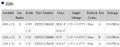
The PS3 has 256MB of 64 bit bus Rambus XDR main system memory. | == Chipnumers @ SKU's == | ||
The PS3 has 256MB of 64 bit bus Rambus XDR main system memory. Older models use four 64MB chips, while newer models uses two 128MB chips. | |||
{|class="wikitable" | |||
|- | |||
|- | ! PS3 Model !! Mobo Model !! Mobo serial !! RAM Serial !! Amount !! Notes | ||
|- | |||
| [[CECHAxx]] || [[COK-00x#COK-001|COK-001]] || 1-871-868-12<br />1-871-868-22<br />1-871-868-32 || [[X5116ACSE-3C-E]]<br /> or<br />[[K4Y50164UC-JCB3 ]] || style="text-align:center;" | 4 || | |||
|- | |||
| [[CECHBxx]] || [[COK-00x#COK-001|COK-001]] || 1-871-868-12<br />1-871-868-22<br />1-871-868-32 || [[X5116ACSE-3C-E]]<br /> or<br />[[K4Y50164UC-JCB3 ]] || style="text-align:center;" | 4 || | |||
|- | |||
| [[CECHCxx]] || [[COK-00x#COK-002|COK-002]] || 1-873-513-21<br />1-873-513-31 || [[X5116ACSE-3C-E]]<br /> or<br />[[K4Y50164UC-JCB3 ]] || style="text-align:center;" | 4 || | |||
|- | |||
| style="text-align:center; background-color:lightgrey;" | <span style="background-color:lightgrey;">[[CECHDxx]]</span> || colspan="6" style="text-align:center; background-color:lightgrey;" | <span style="background-color:lightgrey;">SKU never released</span> | |||
|- | |||
| [[CECHExx]] || [[COK-00x#COK-002W|COK-002W]] || || [[X5116ACSE-3C-E]]<br /> or<br />[[K4Y50164UC-JCB3 ]] || style="text-align:center;" | 4 || | |||
|- | |||
| style="text-align:center; background-color:lightgrey;" | <span style="background-color:lightgrey;">[[CECHFxx]]</span> || colspan="6" style="text-align:center; background-color:lightgrey;" | <span style="background-color:lightgrey;">SKU never released</span> | |||
|- | |||
| [[CECHGxx]] || [[SEM-00x|SEM-001]] || 1-875-384-21<br />1-875-384-31 || [[X5116ACSE-3C-E]] || style="text-align:center;" | 4 || | |||
|- | |||
| [[CECHHxx]] || [[DIA-00x#DIA-001|DIA-001]] || 1-875-368-11<br />1-875-368-31 || [[X5116ADSE-3C-E]] || style="text-align:center;" | 4 || | |||
|- | |||
| style="text-align:center; background-color:lightgrey;" | <span style="background-color:lightgrey;">[[CECHIxx]]</span> || colspan="6" style="text-align:center; background-color:lightgrey;" | <span style="background-color:lightgrey;">SKU never released</span> | |||
|- | |||
| [[CECHJxx]] || [[DIA-00x#DIA-002|DIA-002]] || 1-876-912-32 || [[K4Y50164UE-JCB3]] || style="text-align:center;" | 4 || | |||
|- | |||
| [[CECHKxx]] || [[DIA-00x#DIA-002|DIA-002]] || 1-876-912-32 || [[K4Y50164UE-JCB3]] || style="text-align:center;" | 4 || | |||
|- | |||
| [[CECHLxx]] || [[VER-00x|VER-001]] || 1-878-196-31<br />1-878-196-41 || [[X5116ADSE-3C-E]]<br /> or<br />[[IDRD51-0-A1F1C-32C]] || style="text-align:center;" | 4 || | |||
|- | |||
| [[CECHMxx]] || [[VER-00x|VER-001]] || 1-878-196-31<br />1-878-196-41 || [[X5116ADSE-3C-E]] || style="text-align:center;" | 4 || | |||
|- | |||
| style="text-align:center; background-color:lightgrey;" | <span style="background-color:lightgrey;">[[CECHNxx]]</span> || colspan="6" style="text-align:center; background-color:lightgrey;" | <span style="background-color:lightgrey;">SKU never released</span> | |||
|- | |||
| style="text-align:center; background-color:lightgrey;" | <span style="background-color:lightgrey;">[[CECHOxx]]</span> || colspan="6" style="text-align:center; background-color:lightgrey;" | <span style="background-color:lightgrey;">SKU never released</span> | |||
|- | |||
| [[CECHPxx]] || [[VER-00x|VER-001]] || 1-878-196-31<br />1-878-196-41 || [[X5116ADSE-3C-E]] || style="text-align:center;" | 4 || | |||
|- | |||
| [[CECHQxx]] || [[VER-00x|VER-001]] || 1-878-196-31<br />1-878-196-41 || [[X5116ADSE-3C-E]] || style="text-align:center;" | 4 || | |||
|- | |||
| [[CECH-20xx]] || [[DYN-00x|DYN-001]] || 1-880-055-31 || [[X5116ADSE-3C-E]] || style="text-align:center;" | 4 || | |||
|- | |||
| [[CECH-21xx]] || [[SUR-00x|SUR-001]] || 1-881-945-11 || [[X1032BASE-3C-F]] || style="text-align:center;" | 2 || | |||
|- | |||
| [[CECH-25xx]] || [[JTP-00x|JTP-001]] || 1-882-481-31 || [[X1032BASE-3C-F#Elpida X1032BASE-3CA2-F|X1032BASE-3CA2-F ]] || style="text-align:center;" | 2 || | |||
|- | |||
| [[CECH-25xx]] || [[JSD-00x|JSD-001]] || 1-882-770-11 || [[X1032BASE-3C-F]] || style="text-align:center;" | 2 || | |||
|- | |||
| [[CECH-30xx]] || [[KTE-00x|KTE-001]] || 1-884-749-11 || [[X1032BASE-3C-F]] || style="text-align:center;" | 2 || | |||
|- | |- | ||
| | | [[CECH-40xx]] || [[MSX-00x|MSX-001]] || 1-886-928-11 || [[X1032BBBG-3C-F]] || style="text-align:center;" | 2 || | ||
|- | |- | ||
| | | [[CECH-40xx]] || [[MPX-00x|MPX-001]] || 1-887-233-11 || [[X1032BBBG-3C-F]] || style="text-align:center;" | 2 || | ||
|- | |- | ||
| | | [[CECH-42xx]] || [[NPX-00x|NPX-001]] || 1-887-357-11 || [[X1032BBBG-3C-F]] || style="text-align:center;" | 2 || | ||
|- | |- | ||
| | | [[CECH-42xx]] || [[PQX-00x|PQX-001]] || 1-888-629-11 || [[X1032BBBG-3C-F]] || style="text-align:center;" | 2 || | ||
|- | |- | ||
| | | [[CECH-43xx]] || [[REX-00x|REX-001]] || 1-893-507-31 || [[K4Y12324TE-KCB3]] || style="text-align:center;" | 2 || | ||
|- | |- | ||
|} | |} | ||
< | <gallery> | ||
File:Elpida XDR DRAM on production at June 4, 2013.jpg|Elpida XDR DRAM on production at June 4, 2013 | |||
File:Elpida XDR DRAM out of production at June 4, 2013.jpg|Elpida XDR DRAM out of production at June 4, 2013 | |||
</gallery> | |||
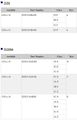
=== Alternate table === | |||
{| border="1" cellspacing="0" cellpadding="5" border="#999" class="wikitable" style="border:1px solid #999; border-collapse: collapse;" | |||
|- bgcolor="#cccccc" | |||
! Type !! Size !! Speed !! Voltage !! Packaging !! Manufact. !! Serial Number !! Amount !! Models | |||
|- | |||
| Rambus XDR || 64MB || 400MHz || 1.8V+/-0.09V || FBGA-104 || Elpida || [[X5116ACSE-3C-E]] || 4x || [[CECHAxx]]/[[COK-00x#COK-001|COK-001]] up to including [[CECHGxx]]/[[SEM-00x|SEM-001]] | |||
|- | |||
| Rambus XDR || 64MB || 400MHz || 1.8V+/-0.09V || FBGA-104 || Samsung || [[K4Y50164UC-JCB3]] || 4x || ?Some initial models? | |||
|- | |||
| Rambus XDR || 64MB || 400MHz || 1.8V+/-0.09V || FBGA-100 || Samsung || [[K4Y50164UE-JCB3]] || 4x || [[CECHJxx]]/[[DIA-00x#DIA-002|DIA-002]] and [[CECHKxx]]/[[DIA-00x#DIA-002|DIA-002]] | |||
|- | |||
| Rambus XDR || 64MB || 400MHz || 1.8V+/-0.09V || FBGA-104 || Elpida || [[X5116ADSE-3C-E]] || 4x || [[CECHHxx]]/[[DIA-00x#DIA-001|DIA-001]], [[CECHLxx]]/[[VER-00x|VER-001]] up and including [[CECHQxx]]/[[VER-00x|VER-001]] and PS3 Slim [[CECH-20xx]]/[[DYN-00x|DYN-001]] | |||
|- | |||
| Rambus XDR || 64MB || 400MHz || 1.8V+/-0.09V || FBGA-104 || Qimonda || [[IDRD51-0-A1F1C-32C]] || 4x || reported on some [[CECHLxx]]/[[VER-00x|VER-001]] | |||
|- | |||
| Rambus XDR || 128MB || 400MHz || 1.5V+/-0.075V || FBGA-150 || Elpida || [[X1032BASE-3C-F]] || 2x || [[CECH-21xx]]/[[SUR-00x|SUR-001]] and newer | |||
|- | |||
|} | |||
=== | == Other XDR Rambus references == | ||
* [https://www-01.ibm.com/chips/techlib/techlib.nsf/techdocs/AF7832F379790768872572D10047E52B/$file/CellBE_HIG_65nm_v1.01_8Jun2007.pdf CellBE_HIG_65nm_v1.01_8Jun2007.pdf] | |||
* [http://www.capsl.udel.edu/~jmanzano/Cell/docs/arch/BE_Hardwar_Init_Guide_v1.3_31March2006.pdf BE_Hardwar_Init_Guide_v1.3_31March2006.pdf] | |||
* [http://www.rambus.com/assets/documents/products/dl_0362_v0_71.pdf Rambus XDR IO Cell (XIO) - dl_0362_v0_71.pdf] | |||
* [http://www.rambus.com/assets/documents/products/dl_0161_v0_8.pdf XDR Architecture - Rambus dl_0161_v0_8.pdf] | |||
* [http://www.rambus.com/assets/documents/products/xdr_dl_0476.pdf 8x4Mx16/8/4/2 - Rambus xdr_dl_0476.pdf] | |||
* [http://www.rambus.com/assets/documents/products/dl_0169l_v0_81.pdf XDR Clock Generator - Rambus dl_0169l_v0_81.pdf] | |||
* dl_0178_v0_93.pdf (january 2006) | |||
* dl_0178_v0_95.pdf (august 2006) | |||
* http://www.mirrorcreator.com/files/1KD96OYT/xdr_product_guide_mar_06_0.pdf_links | |||
* http://www.mirrorcreator.com/files/1C1NTTYD/Elpida_E1819E20_0.pdf_links | |||
* http://www.mirrorcreator.com/files/KGNOVWHK/Elpida_E0881E20_0.pdf_links | |||
* http://www.mirrorcreator.com/files/SSF2GNEK/Samsung_k4y50xx4ue_rev10.pdf_links | |||
* http://www.mirrorcreator.com/files/1FQRE8S5/Samsung_k4y50xx4uc_rev11_0.pdf_links | |||
* http://www.mirrorcreator.com/files/11S5L1EW/Elpida_E1033E40_EOL_0.pdf_links | |||
= Video Memory (VRAM) = | |||
<div style="float:right">[[File:GDDR3 to RSX to CellBE diagram.png|200px|thumb|left|Quad 64MB GDDR3 (256MB total) to RSX to CellBE diagram ]]<br />[[File:RSX_MEMORY.jpg|200px|thumb|left|RSX bare die<br />GPU in centre<br />4x GDDR3]]</div> | |||
The 256MB of GDDR3 memory is located inside the [[RSX]] chip using four 64MB FBGA chips. | |||
The 256MB of GDDR3 memory is located inside the RSX chip using four 64MB FBGA chips. | |||
{| border="1" cellspacing="0" cellpadding="5" border="#999" class="wikitable" style="border:1px solid #999; border-collapse: collapse;" | {| border="1" cellspacing="0" cellpadding="5" border="#999" class="wikitable" style="border:1px solid #999; border-collapse: collapse;" | ||
|- bgcolor="#cccccc" | |- bgcolor="#cccccc" | ||
! Type !! Size !! Speed !! Voltage !! Packaging !! Manufacturer !! Serial Number !! Description | ! Type !! Size !! Speed !! Voltage !! Packaging !! Manufacturer !! Serial Number !! Description | ||
|- | |- | ||
| GDDR3 || 64MB (512Mbit) || 700MHz || 2.0V +/-0.1V || <strike>FBGA-136</strike> on-die || Samsung || K4J52324QC-SC14 || 256MB total (4 chips) for PS3 Graphics Memory | | GDDR3 || 64MB (512Mbit) || 700MHz || 2.0V +/-0.1V || <strike>FBGA-136</strike> on-die || Samsung || [[K4J52324QC-SC14]] || 256MB total (4 chips) for PS3 Graphics Memory | ||
|- | |||
| GDDR3 || 64MB (512Mbit) || 700MHz || 2.0V +/-0.1V || <strike>FBGA-136</strike> on-die || Infineon/Qimonda || [[HYB18H512322AF-14]] || 256MB total (4 chips) for PS3 Graphics Memory | |||
|- | |||
| GDDR3 || 64MB (512Mbit) || ? || ? || ? || Samsung || [[K4J52324KI-JC14]] || 256MB total (4 chips) for PS3 Graphics Memory | |||
|- | |||
| GDDR3 || 64MB (512Mbit) || ? || ? || ? || Samsung || [[K4J52324KJ-JC14]] || 256MB total (4 chips) for PS3 Graphics Memory | |||
|- | |- | ||
| GDDR3 || | | GDDR3 || 128MB (1024Mbit) ? || ? || ? || ? || Hynix || [[H5RS5223DFA]] || 256MB total (2 chips ?) for PS3 Graphics Memory | ||
|- | |- | ||
|} | |} | ||
= PS2 Compatibility Memory = | |||
See: [[PS2 Compatibility]] | |||
{{Motherboard Components}}<noinclude>[[Category:Main]]</noinclude> | |||
< | |||
Revision as of 08:09, 14 April 2021
System Memory (RAM)


Chipnumers @ SKU's
The PS3 has 256MB of 64 bit bus Rambus XDR main system memory. Older models use four 64MB chips, while newer models uses two 128MB chips.
Elpida XDR DRAM on production at June 4, 2013
Elpida XDR DRAM out of production at June 4, 2013

Alternate table
| Type | Size | Speed | Voltage | Packaging | Manufact. | Serial Number | Amount | Models |
|---|---|---|---|---|---|---|---|---|
| Rambus XDR | 64MB | 400MHz | 1.8V+/-0.09V | FBGA-104 | Elpida | X5116ACSE-3C-E | 4x | CECHAxx/COK-001 up to including CECHGxx/SEM-001 |
| Rambus XDR | 64MB | 400MHz | 1.8V+/-0.09V | FBGA-104 | Samsung | K4Y50164UC-JCB3 | 4x | ?Some initial models? |
| Rambus XDR | 64MB | 400MHz | 1.8V+/-0.09V | FBGA-100 | Samsung | K4Y50164UE-JCB3 | 4x | CECHJxx/DIA-002 and CECHKxx/DIA-002 |
| Rambus XDR | 64MB | 400MHz | 1.8V+/-0.09V | FBGA-104 | Elpida | X5116ADSE-3C-E | 4x | CECHHxx/DIA-001, CECHLxx/VER-001 up and including CECHQxx/VER-001 and PS3 Slim CECH-20xx/DYN-001 |
| Rambus XDR | 64MB | 400MHz | 1.8V+/-0.09V | FBGA-104 | Qimonda | IDRD51-0-A1F1C-32C | 4x | reported on some CECHLxx/VER-001 |
| Rambus XDR | 128MB | 400MHz | 1.5V+/-0.075V | FBGA-150 | Elpida | X1032BASE-3C-F | 2x | CECH-21xx/SUR-001 and newer |
Other XDR Rambus references
- CellBE_HIG_65nm_v1.01_8Jun2007.pdf
- BE_Hardwar_Init_Guide_v1.3_31March2006.pdf
- Rambus XDR IO Cell (XIO) - dl_0362_v0_71.pdf
- XDR Architecture - Rambus dl_0161_v0_8.pdf
- 8x4Mx16/8/4/2 - Rambus xdr_dl_0476.pdf
- XDR Clock Generator - Rambus dl_0169l_v0_81.pdf
- dl_0178_v0_93.pdf (january 2006)
- dl_0178_v0_95.pdf (august 2006)
- http://www.mirrorcreator.com/files/1KD96OYT/xdr_product_guide_mar_06_0.pdf_links
- http://www.mirrorcreator.com/files/1C1NTTYD/Elpida_E1819E20_0.pdf_links
- http://www.mirrorcreator.com/files/KGNOVWHK/Elpida_E0881E20_0.pdf_links
- http://www.mirrorcreator.com/files/SSF2GNEK/Samsung_k4y50xx4ue_rev10.pdf_links
- http://www.mirrorcreator.com/files/1FQRE8S5/Samsung_k4y50xx4uc_rev11_0.pdf_links
- http://www.mirrorcreator.com/files/11S5L1EW/Elpida_E1033E40_EOL_0.pdf_links
Video Memory (VRAM)


The 256MB of GDDR3 memory is located inside the RSX chip using four 64MB FBGA chips.
| Type | Size | Speed | Voltage | Packaging | Manufacturer | Serial Number | Description |
|---|---|---|---|---|---|---|---|
| GDDR3 | 64MB (512Mbit) | 700MHz | 2.0V +/-0.1V | Samsung | K4J52324QC-SC14 | 256MB total (4 chips) for PS3 Graphics Memory | |
| GDDR3 | 64MB (512Mbit) | 700MHz | 2.0V +/-0.1V | Infineon/Qimonda | HYB18H512322AF-14 | 256MB total (4 chips) for PS3 Graphics Memory | |
| GDDR3 | 64MB (512Mbit) | ? | ? | ? | Samsung | K4J52324KI-JC14 | 256MB total (4 chips) for PS3 Graphics Memory |
| GDDR3 | 64MB (512Mbit) | ? | ? | ? | Samsung | K4J52324KJ-JC14 | 256MB total (4 chips) for PS3 Graphics Memory |
| GDDR3 | 128MB (1024Mbit) ? | ? | ? | ? | Hynix | H5RS5223DFA | 256MB total (2 chips ?) for PS3 Graphics Memory |
PS2 Compatibility Memory
See: PS2 Compatibility
| |||||||||||||||||||||||||||||||||||||||||||||||||||||||||||||||||||||||||||||||||||||||||||||||||||||||||||||||||||||||||||||||||||||||||||||||||||||||||||||||||||||||||||||
