CELL BE
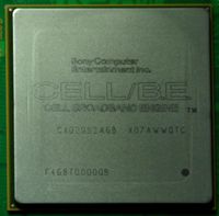
Cell Broadband Engine
The Cell CPU has one 3.2Ghz PPE (Power Processor Element) with two threads and eight 3.2Ghz SPE (Synergistic Processing Elements).
The PPE is a general purpose CPU, while the eight SPE are geared towards processing data in parallel. One SPE is disabled to increase yield, so the PS3 can have at most 9 threads running at the same time (2 from PPE and 7 from SPE). Note that one SPE is reserved for the hypervisor, so PS3 programs can take advantage of 8 threads. Both the PPE and SPE of the Cell are 64 bit, and manipulate data in Big Endian.
Specifications
- 1 PPE (Power Processor Element)
- 3.2Ghz
- 64 bit, Big Endian
- 2 threads (can run at same time)
- L1 cache: 32kB data + 32kB instruction
- L2 cache: 512kB
- Memory bus width: 64bit (serial)
- VMX (Altivec) instruction set support
- Full IEEE-754 compliant
- the PPU can execute two double precision or eight single precision operations per clockcycle
- 8 SPE (Synergistic Processing Element)
- 3.2Ghz
- 64 bit, Big Endian
- 1 SPE disabled to improve chip yield (see: Unlocking the 8th SPE)
- 1 SPE dedicated for hypervisor security
- 256KB local store per SPE
- 128 registers per SPE
- Dual Issue (Each SPE can execute 2 instructions per clock)
- IEEE-754 compliant in double precision (single precision round-towards-zero instead of round-towards-even)
There is a lot of info about CELL/BE on the Cell Programming IBM page.
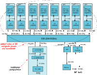
Die explained
| ABBR | Usage | Speed | Notes |
|---|---|---|---|
| BEI | Broadband engine interface | 1.6GHz (NCLK/2) | I/O Controller to FlexIO(/RSX) |
| EIB | Element interconnect bus | 1.6GHz (NCLK/2) | used as communication ring for the 8 SPE (and PPU + MIC + BEI) |
| FlexIO | High-speed I/O interface | 2.5Ghz (RC_REFCLK : 500MHz 1:5 PLL) | Flex I/O to RSX |
| L2 | Level 2 cache | 3.2GHz (NCLK) | 512KB L2 cache for PPE |
| MIC | Memory interface controller | 1.6GHz (NCLK/2) | Memory controller to XIO(/Rambus XDR) |
| MBL | MIC bus logic | 1.6GHz (NCLK/2) | From MIC(/PPE) to EIB(/SPE's) |
| PPE | Power processor element | 3.2GHz (NCLK) | Main dualthreaded CPU |
| SPE | Synergistic processor element | 3.2GHz/1.6GHz | 8 present, 1 disabled from factory |
| XIO | Extreme data rate I/O cell | 1.6GHz (Y0_RQ_CTM/Y1_RQ_CTM : 400MHz 1:4 PLL) | Rambus XDR Interface |
| TEST | Test control unit (TCU) / pervasive logic (PRV) | Used for power management, thermal management, clock control, software-performance monitoring, trace analysis, preboot (and secureboot?), also has RAS-unit (Reliability, Availability, Serviceability), JTAG (IEEE 1149 test access port) and SPI Serial Peripheral Interface | |
| PLL | Phase-Locked Loop | 400MHz | Before preboot external clock (400MHz) is used (see Timebases) afterwards only internal PLL (PLL_REFCLK : 400MHz 1:8 PLL) for main clocks: NCLK=3.2GHz, NCLK/2=1.6GHz, MiClk=1.6GHz, XIO Clk=1.6GHz, BClk=1.667GHz, RO/TO Clk=2.5GHz |
SPE
| ABBR | Usage | Speed | Notes |
|---|---|---|---|
| BIU | Bus interface unit | 1.6GHz (NCLK/2) | connects DMAC+EIB and LS+EIB |
| DMAC | Direct memory access controller | 1.6GHz (NCLK/2) | controls DMA, SPU+LS and BIU(/EIB) |
| EIB | Element interconnect bus | 1.6GHz (NCLK/2) | busring to which all SPE's are connected (and PPU + MIC + BEI) |
| LS | Local store | 3.2GHz (NCLK) | 256KB of local memory, accessable via DMA/MBOX |
| MFC | Memory flow controller | 1.6GHz (NCLK/2) | |
| MIC | Memory interface controller | 1.6GHz (NCLK/2) | Memory controller to XIO(/Rambus XDR) |
| MMIO | Memory-mapped I/O | 1.6GHz (NCLK/2) | |
| MMU | Memory management unit | 1.6GHz (NCLK/2) | used by DMAC for management |
| SPU | Synergistic processor unit | 3.2GHz (NCLK) | SPU execution unit |
| TLB | Translation lookaside buffer | 1.6GHz (NCLK/2) | used by MMU as buffer |
Reference: http://hpc.pnl.gov/people/fabrizio/papers/ieeemicro-cell.pdf // backup/mirror: ieeemicro-cell.pdf (222.51 KB)
Bandwidth I/O
- MIC (Memory Interface Controller) <from/to> dual Rambus XDR: 25.6GB/s theoretical
- IOIF0 (I/O Interface to RSX): 20GB/s to> RSX / 15 GB/s < RSX (RSX <from/to> GDDR3: 20.8GB/s @ 650MHz)
- IOIF1 (I/O Interface to Southbridge): <from/to> South Bridge : 2.5GB/s
- EIB (Element Interconnect Bus) : 4x 128bit buses / 128byte packets : 204.8 GB/s total
- PPU (PowerPC Processing Element) : 25.6 GLOP/s FPU, L1/L2: 51.2GB/s
- LHS (Load Hit Store) pipeline stall : ~40 clockcycles
- SPE (Synergistic Processor Elements) : 2 IPC SPU to Local Store : 51.2GB/s
Reference: Cell Broadband Engine Architecture and its first implementation - A performance view
Serial Numbers @ SKU
Note: All Cell BE packages measures 42.5mm × 42.5mm
The Cell BE was introduced at 90nm. Later, PS3 model numbers starting with CECHG uses the 65nm version, while the PS3 Slim (CECH-20xx) used the 45nm version (See SKU Models and table below).
A sampling of the serial numbers by model number:
| PS3 Model | Mobo Model | Mobo serial | CELL Serial | Die Tech | Total Die Size | Width x Length | SPU size | PPE Size | Remark |
|---|---|---|---|---|---|---|---|---|---|
| CECHAxx | COK-001 | - | CXD2964GB | 90nm | 235.48mm² | 19.17mm x 12.29mm | 14.76mm² | 28.86mm² | edepot ps3secrets |
| CECHAxx | COK-001 | 1-871-868-12 | CXD2964AGB | 90nm | 235.48mm² | 19.17mm x 12.29mm | 14.76mm² | 28.86mm² | reballing.es |
| CECHAxx | COK-001 | 1-871-868-22 | CXD2964GB | 90nm | 235.48mm² | 19.17mm x 12.29mm | 14.76mm² | 28.86mm² | reballing.es |
| CECHAxx | COK-001 | 1-871-868-32 | CXD2964GB | 90nm | 235.48mm² | 19.17mm x 12.29mm | 14.76mm² | 28.86mm² | reballing.es |
| CECHBxx | COK-001 | - | CXD2964GB | 90nm | 235.48mm² | 19.17mm x 12.29mm | 14.76mm² | 28.86mm² | edepot ps3secrets |
| CECHBxx | COK-001 | 1-871-868-22 | CXD2964GB | 90nm | 235.48mm² | 19.17mm x 12.29mm | 14.76mm² | 28.86mm² | reballing.es |
| CECHBxx | COK-001 | 1-871-868-32 | CXD2964GB | 90nm | 235.48mm² | 19.17mm x 12.29mm | 14.76mm² | 28.86mm² | reballing.es |
| CECHCxx | COK-002 | 1-873-513-21 1-873-513-31 |
CXD2964GB | 90nm | 235.48mm² | 19.17mm x 12.29mm | 14.76mm² | 28.86mm² | edepot ps3secrets |
| CECHExx | COK-002W | - | CXD29?? | 90nm | 235.48mm² | 19.17mm x 12.29mm | 14.76mm² | 28.86mm² | edepot ps3secrets |
| CECHExx | COK-002W | 1-873-513-21 | CXD2964GB | 90nm | 235.48mm² | 19.17mm x 12.29mm | 14.76mm² | 28.86mm² | reballing.es |
| CECHExx | COK-002W | 1-873-513-21 | CXD2964AGB | 90nm | 235.48mm² | 19.17mm x 12.29mm | 14.76mm² | 28.86mm² | reballing.es |
| CECHExx | COK-002W | 1-873-513-31 | CXD2964AGB | 90nm | 235.48mm² | 19.17mm x 12.29mm | 14.76mm² | 28.86mm² | reballing.es |
| CECHExx | COK-002W | 1-873-513-31 | CXD2964GB | 90nm | 235.48mm² | 19.17mm x 12.29mm | 14.76mm² | 28.86mm² | reballing.es |
| CECHGxx | SEM-001 | 1-875-384-11 1-875-384-21 1-875-384-31 |
CXD2981AGB | 65nm | 174.61mm² | 15.59mm x 11.20mm | 11.08mm² | 19.60mm² | edepot ps3secrets |
| CECHHxx | DIA-001 | 1-875-368-11 1-875-368-31 |
CXD2981GB | 65nm | 174.61mm² | 15.59mm x 11.20mm | 11.08mm² | 19.60mm² | edepot ps3secrets |
| CECHHxx | DIA-001 | 1-875-938-11 | CXD2981AGB | 65nm | 174.61mm² | 15.59mm x 11.20mm | 11.08mm² | 19.60mm² | reballing.es |
| CECHHxx | DIA-001 | 1-875-938-31 | CXD2981AGB | 65nm | 174.61mm² | 15.59mm x 11.20mm | 11.08mm² | 19.60mm² | reballing.es |
| CECHJxx | DIA-002 | 1-876-912-31 | CXD2989GB | 65nm | 174.61mm² | 15.59mm x 11.20mm | 11.08mm² | 19.60mm² | edepot ps3secrets |
| CECHKxx | DIA-002 | 1-876-912-32 | CXD2989AGB | 65nm | 174.61mm² | 15.59mm x 11.20mm | 11.08mm² | 19.60mm² | edepot ps3secrets |
| CECHKxx | DIA-002 | 1-876-912-32 | CXD2990GB | 65nm | 174.61mm² | 15.59mm x 11.20mm | 11.08mm² | 19.60mm² | |
| CECHLxx | VER-001 | - | CXD2990AGB | 65nm | 174.61mm² | 15.59mm x 11.20mm | 11.08mm² | 19.60mm² | edepot ps3secrets |
| CECHLxx | VER-001 | 1-878-196-31 | CXD2990GB | 65nm | 174.61mm² | 15.59mm x 11.20mm | 11.08mm² | 19.60mm² | reballing.es |
| CECHMxx | VER-001 | ?1-878-196-41? | -? | 65nm | 174.61mm² | 15.59mm x 11.20mm | 11.08mm² | 19.60mm² | -? |
| CECHPxx | VER-001 | ?1-878-196-41? | -? | 65nm | 174.61mm² | 15.59mm x 11.20mm | 11.08mm² | 19.60mm² | -? |
| CECHQxx | VER-001 | ?1-878-196-41? | CXD299? | 65nm | 174.61mm² | 15.59mm x 11.20mm | 11.08mm² | 19.60mm² | edepot ps3secrets |
| CECH-20xx | DYN-001 | - | CXD2992AGB | 45nm | 115.46mm² | 12.75mm x 9.06mm | 6.47mm² | 11.32mm² | edepot ps3secrets |
| CECH-20xx | DYN-001 | 1-880-055-31 | CXD2992AGB | 45nm | 115.46mm² | 12.75mm x 9.06mm | 6.47mm² | 11.32mm² | reballing.es |
| CECH-21xx | SUR-001 | - | CXD2992AGB | 45nm | 115.46mm² | 12.75mm x 9.06mm | 6.47mm² | 11.32mm² | edepot ps3secrets |
| CECH-21xx | SUR-001 | 1-881-945-11 | CXD2992AGB | 45nm | 115.46mm² | 12.75mm x 9.06mm | 6.47mm² | 11.32mm² | reballing.es |
| CECH-25xx | JTP-001 | 1-882-481-21 | CXD2992GB | 45nm | 115.46mm² | 12.75mm x 9.06mm | 6.47mm² | 11.32mm² | |
| CECH-25xx | JTP-001 | 1-882-481-31 | CXD2992GB | 45nm | 115.46mm² | 12.75mm x 9.06mm | 6.47mm² | 11.32mm² | edepot ps3secrets |
| CECH-25xx | JSD-001 | 1-882-770-11 | CXD2992BGB | 45nm | 115.46mm² | 12.75mm x 9.06mm | 6.47mm² | 11.32mm² | |
| CECH-25xx | JSD-001 | 1-882-770-21 | CXD2992GB | 45nm | 115.46mm² | 12.75mm x 9.06mm | 6.47mm² | 11.32mm² | |
| CECH-30xx | KTE-001 | 1-884-749-11 | CXD2996GB? | 45nm? | 115.46mm²? | 12.75mm x 9.06mm? | 6.47mm²? | 11.32mm²? | -? |
| CECH-30xx | KTE-001 | 1-884-749-31 | CXD2996GB | 45nm | 115.46mm² | 12.75mm x 9.06mm | 6.47mm² | 11.32mm² | |
| CECH-40xx | MSX-001 | 1-886-928-11 | CXD2996BGB | 45nm? | 115.46mm²? | 12.75mm x 9.06mm? | 6.47mm²? | 11.32mm²? | techrepublic |
| CECH-40xx | MPX-001 | 1-887-233-11 | CXD2996BGB | 45nm? | 115.46mm²? | 12.75mm x 9.06mm? | 6.47mm²? | 11.32mm²? | -? |
| ? | NPX-001 | ? | ? | 45nm? | 115.46mm²? | 12.75mm x 9.06mm? | 6.47mm²? | 11.32mm²? | -? |
| ? | PPX-001 | ? | ? | ?nm (smaller ?) | ?mm² | ?mm x ?mm | ?mm² | ?mm² | |
| CECH-42xx | PQX-001 | 1-888-629-22 | CXD2999AGG | ?nm (smaller ?) | ?mm² | ?mm x ?mm | ?mm² | ?mm² | mobile01_tw |
| ? | RTX-001 | ? | ? | ?nm (smaller ?) | ?mm² | ?mm x ?mm | ?mm² | ?mm² | |
| ? | REX-001 | ? | ? | ?nm (smaller ?) | ?mm² | ?mm x ?mm | ?mm² | ?mm² |
Alternative listing
- CXD2964 series (90nm)
- CXD2981 series (65nm)
- CXD2989 series (65nm)
- CXD2990 series (65nm)
- CXD2992 series (45nm)
- CXD2992GB, found in: CECH-25xx/JTP-001 and CECH-25xx/JSD-001 (without the black plastic spacer in between the IHS and the substrate. Standard thermal paste in the DIE)
- CXD2992AGB, found in: CECH-20xx/DYN-001, CECH-21xx/SUR-001
- CXD2992BGB, found in: CECH-25xx/JTP-001 and CECH-25xx/JSD-001 (with the black plastic spacer in between the IHS and the substrate. Posible thermal adhesive in the DIE)
- CXD2996 series (45nm)
- CXD2999 series (?? nm)
- CXD2999AGG, found in: CECH-42xx/PQX-001
PVR (powerpc version register)
The PVR inside the microprocessor is the only way to identify what version of what part you have.
cat /proc/cpuinfo
or
  unsigned int pvr;
  __asm__ __volatile__ ("mfpvr %0" : "=r" (pvr));
code above should work in kernel & user mode.
| CellBE serial | die tech | PVR | Notes |
|---|---|---|---|
| CXD2964AGB | 90nm | ||
| CXD2964GB | 90nm | ||
| CXD2981AGB | 65nm | ||
| CXD2981GB | 65nm | ||
| CXD2989AGB | 65nm | ||
| CXD2989GB | 65nm | ||
| CXD2990AGB | 65nm | ||
| CXD2990GB | 65nm | ||
| CXD2992AGB | 45nm | ||
| CXD2992GB | 45nm | ||
| CXD2996GB | 45nm | ||
| CXD2999AGG |
Cell Revisions
| Low word of BP_VR | Revision | Name |
|---|---|---|
| 0x0000 | 0x010 | 90 nm DD 1.0 |
| 0x0001 | 0x011 | 90 nm DD 1.1 |
| 0x0002 | 0x012 | 90 nm DD 1.2 |
| 0x0100 | 0x020 | 90 nm DD 2.0 |
| 0x0200 | 0x030 | 90 nm DD 3.0 |
| 0x0201 | 0x031 | 90 nm DD 3.1 |
| 0x0202 | 0x032 | 90 nm DD 3.2 |
| 0x1000 | 0x110 | 65 nm DD 1.0 |
| 0x2000 | 0x210 | 45 nm DD 1.0 |
| 0x2100 | 0x220 | 45 nm DD 2.0 |
| CellBE Version | PVR | Speed | SKU |
|---|---|---|---|
| Cell/BE v1.0 | 0x0070 0x0100 | 2.4GHz | CEB-1020 |
| Cell/BE v2.0 | 0x0070 0x0400 | 2.4GHz | CEB-2030, CEB-2040 |
| Cell/BE v3.0 | 0x0070 0x0500 | 3.2GHz | CEB-2050 |
| Cell/BE v3.1 | 0x0070 0x0501 | 3.2GHz | CEB-9000 |
| Cell/BE v3.2 | 0x0070 0x0501 | 3.2GHz | |
| ???? | 0x0070 0x2100 |
Unsorted
Cell Integrated Heat Spreader (IHS) WARNING
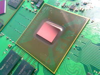
Starting with PS3 Slim models CECH-25xx some of the CELL Integrated Heat Spreaders are secured to the CELL processor die with thermal adhesive. Cell processor models with a thinner substrate and black plastic spacer in between the IHS and the substrate may be glued. Removing an IHS that is glued to the Cell will destroy the Cell CPU.
Integrated Heat Spreader (IHS) removed pic's
- when it goes OK:
- when it goes wrong:
IHS size and mounting
on a COK-001 the CPU heatspreader is 4.00cm x 4.00cm while the RSX heatspreader is 4.25cm x 4.25 cm - CPU and RSX mountholes are 8.75cm apart and 6.3mm diameter
although a PC cooler should fit within these dimensions fine, mounting the 2 (which are also elevated differently from the motherboard) can be problematic
IHSBuster tool
| |||||||||||||||||||||||||||||||||||||||||||||||||||||||||||||||||||||||||||||||||||||||||||||||||||||||||||||||||||||||||||||||||||||||||||||||||||||||||||||||||||||||||||||


