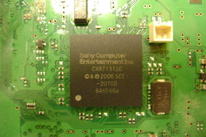
Syscon Hardware
Syscon is the main power controller chip. It is responsible for powering up the various power systems and for configuring and initialising the CELL BE, RSX and South Bridge. It communicates with these devices via seperate SPI busses. There is external access by JTAG (disabled at factory by blowing a fuse), an EEPROM programming interface and Serial (UART). The Syscon is a SoC and consists of an ARM7TDMI (ARMv4) CPU, a 256KB EEPROM and 16KB RAM.
Serialnumbers @ SKU
Retail
| Model | Type | Board | Syscon part no. |
Syscon Soft ID |
Notes |
|---|---|---|---|---|---|
| CECHAxx CECHBxx |
0x01 0x02 |
COK-001 | CXR713120-201GB | 0B8E | |
| CECHCxx CECHExx |
0x03 0x04 |
COK-002 or COK-002W |
CXR713120-201GB or CXR713120-202GB |
0C16 | |
| CECHGxx | 0x05 | SEM-001 | CXR713120-201GB or CXR713120-202GB or CXR713120-203GB |
0D52 | |
| CECHHxx | 0x06 | DIA-001 | CXR714120-301GB | 0DBF | |
| CECHJxx CECHKxx |
0x07 | DIA-002 | CXR714120-301GB or CXR714120-302GB |
0E69 | |
| CECHLxx CECHMxx CECHPxx CECHQxx |
0x08 | VER-001 | SW-301 or SW-302 |
065D | |
| CECH-20xx | 0x09 | DYN-001 | SW2-301 | 0832 | |
| CECH-21xx | 0x0A | SUR-001 | SW2-301 or SW2-302 |
08A0 | |
| CECH-25xx | 0x0B | JTP-001 or JSD-001 |
SW2-301 or SW2-302 or SW2-303 |
08C2 | |
| CECH-30xx | 0x0C | KTE-001 | SW2-301 or SW2-302 or SW2-303 |
0918 | |
| CECH-40xx | 0x0D | MSX-001 or MPX-001 |
SW3-302 | 098F |
Non retail
| Model | Type | Board | Syscon part no. |
Syscon Soft ID |
Active JTAG | Notes |
|---|---|---|---|---|---|---|
| CEB-2040 | - | MPU-501 | CXR713F120GB-000 | Yes | Retail prototype | |
| DECR1000(A/J) | 0x01 | TMU-520 | CXR713F120A | 03FB | ? | Reference tool |
| DEH-H1000A(S)(-E(S)) | 0x01 | COK-001 (Prototype) | CXR713F120A | 0B67 | ? | Preproduction |
| DEH-H1001-D | 0x01 | COOKIE-13 | CXR713F120A | ?0B67? | ? | Preproduction |
| DEH-FH1500J-A | VERTIGO-02 | Preproduction |
Not mentioned:
0F29 - ?
0F38 - ?
Syscon Externalised Ports
Note: for more specific information per model, see the links to each subppage in the Serialnumbers @ SKU table.
Syscon UART packets
SCUART daemon (SCUARTD) packet structure
SCUARTD packets includes header of 0x3 bytes and optional payload (depending on the command). Packet IDs are not important, they are used only by clients and processed by SCUART daemon.
| Offset | Size | Description |
|---|---|---|
| 0x00 | 0x01 | Magic? |
| 0x01 | 0x01 | Payload size |
| 0x02 | 0x01 | Command |
| 0x03 | Payload size | Payload data |
Packets
| Packet ID | Command | Description | Notes |
|---|---|---|---|
| 0x00 | version | ||
| 0x01 | bringup | ||
| 0x02 | shutdown | ||
| 0x03 | firmud | Firmware update | It actually notifies syscon for starting a firmware update operation and calls SX program which implements ZMODEM protocol for transfer |
| 0x04 | bsn | ||
| 0x05 | halt | ||
| 0x06 | cp ready | ||
| 0x07 | cp busy | ||
| 0x08 | cp reset | ||
| 0x09 | bestat |
Real syscon packets have an ASCII form instead of bytes above. An implementation of *MODEM transfer protocols used by Sony: https://github.com/jnavila/lrzsz/tree/master/src
Syscon UART
| BGA | Name | Description |
|---|---|---|
| P16 | UART0_TxD | Serial Transmit |
| P15 | UART0_RxD | Serial Receive |
You can attach a 3.3v TTL cable (LV-TTL) to the UART on syscon (UART0_TxD, UART0_RxD). Baud rate is 57600. There is a simple plaintext protocol involved. This varies on different syscon models. Example:
<command>:<hash>
Where the hash is the sum of command bytes & 0xFF
you should terminate commands with \r\n, the syscon messages are only terminated with \n
Here are some of the commands/messages encountered:
Messages:
Power applied (standby mode)
OK 00000000:3A

Power on
# (PowerOn State):7F

Power off (Hard shutdown)
# (PowerOff State):DD

After Fan test:
# (PowerOff State) (Fatal):36

No text, invalid hash:
NG F0000002:4D

Commands:
VER:ED
OK 00000000 S1E 00 00 065D:A4

ERRLOG:CB
OK 00000000:3A

DATE:1E
NG F0000003:4E
- More info:
Syscon (SPI) EEPROM
| BGA | Name | Description |
|---|---|---|
| F16 | CSB | Chip Select (needs to be low) |
| H16 | DO | Serial Data Output |
| G16 | DI | Serial Data Input |
| E16 | SKB | Serial Data Clock |
| J15 | WCB | Write Protect |
| J16 | RBB | Ready/Busy |
| G11 | VDDep | + 3.3V |
| C15 | VSSep | GND |
Syscon JTAG
disabled in factory after production on retailmodels
| BGA | Name | Description |
|---|---|---|
| L8 | JRTCK | Return Test Clock |
| K8 | JTCK | Test Clock |
| K9 | JTDO | Test Data Out |
| L9 | JTMS | Test Mode State / Test Mode Select |
| K7 | JTDI | Test Data In |
| L7 | JNTRST | Test Reset |
Syscon Underlaying ports
Syscon Cell SPI Bus
| BGA | Name | Description |
|---|---|---|
| M2 | /BE_SPI_CS | Chip Select |
| N2 | BE_SPI_DO | Serial Data Output |
| M1 | BE_SPI_DI | Serial Data Input |
| N1 | BE_SPI_CLK | Serial Data Clock |
| P2 | /BE_RESET | CellBE Reset |
| P1 | BE_POWGOOD | CellBE PowerGood |
| T2 | /BE_INT | CellBE Interrupt |
Syscon Southbridge SPI Bus
| BGA | Name | Description |
|---|---|---|
| B9 | /SB_SPI_CS | Chip Select |
| B8 | SB_SPI_DO | Serial Data Output |
| A9 | SB_SPI_DI | Serial Data Input |
| A8 | SB_SPI_CLK | Serial Data Clock |
| |||||||||||||||||||||||||||||||||||||||||||||||||||||||||||||||||||||||||||||||||||||||||||||||||||||||||||||||||||||||||||||||||||||||||||||||||||||||||||||||||||||||||||||

