PCI: Difference between revisions
Jump to navigation
Jump to search
mNo edit summary |
mNo edit summary |
||
| (One intermediate revision by the same user not shown) | |||
| Line 1: | Line 1: | ||
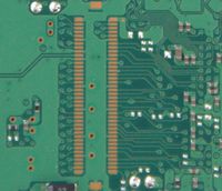
<div style="float:right">[[File:PCI pads - as seen on COK-002.jpg|200px|thumb|left|PCI pads - as seen on COK-002<br>note: Two circular pads in the bottom right corner are for southbridge serial]]< | <div style="float:right">[[File:PCI pads - as seen on COK-002.jpg|200px|thumb|left|PCI pads - as seen on COK-002<br>note: Two circular pads in the bottom right corner are for southbridge serial]]</div> | ||
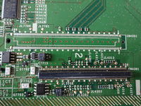
[[File:TMU-520_1-871-645-11_A_Detail_9_(CP_Con.).jpg|200px|thumb|left|Communication Processor (PCI) connector beneath the PCIe x4 connector on a TMU-520]]< | <div style="float:right">[[File:TMU-520_1-871-645-11_A_Detail_9_(CP_Con.).jpg|200px|thumb|left|Communication Processor (PCI) connector beneath the PCIe x4 connector on a TMU-520]]</div> | ||
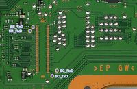
<div style="float:right">[[File:PCI connector JSD-001 SB and SC UART.jpg|200px|thumb|left|PCI connector JSD-001 SB and SC UART]]</div> | |||
== PCI == | == PCI == | ||
| Line 15: | Line 16: | ||
! Device ID !! Device "Name" !! Firmware | ! Device ID !! Device "Name" !! Firmware | ||
|- | |- | ||
| 104D8183 || Sony IFB ATHENS Board Revision 0x1 || [[010.???]] to {{ | | 104D8183 || Sony IFB ATHENS Board Revision 0x1 || [[010.???]] to {{latestPS3}} | ||
|- | |- | ||
| 104D81FF || Sony PIF5 [[TMR-520|TMR]] Board Revision 0x101 || [[0.6.0.004.r010|060.004]] to {{ | | 104D81FF || Sony PIF5 [[TMR-520|TMR]] Board Revision 0x101 || [[0.6.0.004.r010|060.004]] to {{latestPS3}} | ||
|- | |- | ||
| 104D8200 || Sony DVE (RSX Tracing) FPGA || [[0.8.2.006.r010|082.006]] to {{ | | 104D8200 || Sony DVE (RSX Tracing) FPGA || [[0.8.2.006.r010|082.006]] to {{latestPS3}} | ||
|- | |- | ||
| 104D820E || Sony [[CXD9208GP]] PS2 emulation subsystem adapter || [[0.8.2.006.r010|082.006]] to {{ | | 104D820E || Sony [[CXD9208GP]] PS2 emulation subsystem adapter || [[0.8.2.006.r010|082.006]] to {{latestPS3}} | ||
|- | |- | ||
| 80861076 || Intel 82541PI Gigabit Ethernet Controller || [[010.???]] to {{ | | 80861076 || Intel 82541PI Gigabit Ethernet Controller || [[010.???]] to {{latestPS3}} | ||
|- | |- | ||
|} | |} | ||
Latest revision as of 19:56, 16 September 2021
PCI[edit | edit source]
Bus, resembling Conventional PCI 2.3, directly connected to South Bridge, with 80 exposed pads
Activated by setting offset 0x48C02 in SC EEPROM to 0x00 or 0x03:
- 0x00 is for IFB (InterFace Board, used by CEB)
- 0x03 is for Communication Processor (PIF5, used by DEH-R10XX and DECR-1000)
Supported devices:
| Device ID | Device "Name" | Firmware |
|---|---|---|
| 104D8183 | Sony IFB ATHENS Board Revision 0x1 | 010.??? to 4.91 |
| 104D81FF | Sony PIF5 TMR Board Revision 0x101 | 060.004 to 4.91 |
| 104D8200 | Sony DVE (RSX Tracing) FPGA | 082.006 to 4.91 |
| 104D820E | Sony CXD9208GP PS2 emulation subsystem adapter | 082.006 to 4.91 |
| 80861076 | Intel 82541PI Gigabit Ethernet Controller | 010.??? to 4.91 |
Major differences from PCI standard:
- smaller formfactor (80 pin, instead of miniPCI 100P-type I/II or MiniPCI 124P-Type III)
- no use of miniPCI standard sideband signals for audio and communications
- no support of the miniPCI standard CLKRUN# signal defined in the PCI Mobile Design Guide
- no support for optional JTAG signals, nor for the 64-bit PCI extension defined in the PCI Local Bus Specification
70/80 pin miniPCI pad layout[edit | edit source]
CN3208 80P on CECHAxx/CECHBxx COK-001, CECHCxx/CECHExx COK-002(W), CECH-20xx DYN-001 and all later models
CN3208 70P on CECHGxx SEM-001, CECHHxx DIA-001, CECHJxx/CECHKxx DIA-002 and CECHLxx/CECHMxx/CECHPxx/CECHQxx VER-001
| 80P Pin |
70P Pin |
Usage | 100P Pin (Type I/II) |
124P Pin (Type III) |
Remark |
|---|---|---|---|---|---|
| 01 | 35 | +3.3V_PCI | 03, 08, 12, 15, 24, 47, 54, 72, 73 | 19, 24, 28, 31, 40, 63, 70, 88, 89 (not 124) | VCC |
| 02 | 70 | GND | 7, 11, 16, 21, 33, 34, 39, 46, 53, 58, 61, 66, 67, 85, 86, 98 | 23, 27, 32, 37, 49, 50, 55, 62, 69, 74, 77, 82, 83, 101, 102, 114 | Ground |
| 03 | - | PIO15 | ? | ||
| 04 | - | PIO11 | ? | ||
| 05 | - | PIO14 | ? | ||
| 06 | - | PIO10 | ? | ||
| 07 | - | PIO13 | ? | ||
| 08 | - | PIO9 | ? | ||
| 09 | - | PIO12 | ? | ||
| 10 | - | PIO8 | ? | ||
| 11 | 01 | GND | 07, 11, 16, 21, 33, 34, 39, 46, 53, 58, 61, 66, 67, 85, 86, 98 | 23, 27, 32, 37, 49, 50, 55, 62, 69, 74, 77, 82, 83, 101, 102, 114 | Ground |
| 12 | 36 | GND | 07, 11, 16, 21, 33, 34, 39, 46, 53, 58, 61, 66, 67, 85, 86, 98 | 23, 27, 32, 37, 49, 50, 55, 62, 69, 74, 77, 82, 83, 101, 102, 114 | Ground |
| 13 | 02 | /INTA | 04 | 20 | Interrupt line A (open-drain) |
| 14 | 37 | /INTB | 01 | 17 | Interrupt line B (open-drain) |
| 15 | 03 | /INTC | - | - | Interrupt line C (open-drain) |
| 16 | 38 | /INTD | - | - | Interrupt line D (open-drain) |
| 17 | 04 | /RST | 10 | 26 | Reset |
| 18 | 39 | GND | 07, 11, 16, 21, 33, 34, 39, 46, 53, 58, 61, 66, 67, 85, 86, 98 | 23, 27, 32, 37, 49, 50, 55, 62, 69, 74, 77, 82, 83, 101, 102, 114 | Ground |
| 19 | 05 | /GNT | 14 | 30 | Bus grant from motherboard to card |
| 20 | 40 | CLK | 09 | 25 | |
| 21 | 06 | GND | 07, 11, 16, 21, 33, 34, 39, 46, 53, 58, 61, 66, 67, 85, 86, 98 | 23, 27, 32, 37, 49, 50, 55, 62, 69, 74, 77, 82, 83, 101, 102, 114 | Ground |
| 22 | 41 | GND | 07, 11, 16, 21, 33, 34, 39, 46, 53, 58, 61, 66, 67, 85, 86, 98 | 23, 27, 32, 37, 49, 50, 55, 62, 69, 74, 77, 82, 83, 101, 102, 114 | Ground |
| 23 | 07 | /PME | 18 | 34 | Power management event. 3.3 V, open drain, active low |
| 24 | 42 | /REQ | Bus request from card to motherboard | ||
| 25 | 08 | AD30 | 22 | 38 | Address/Data 30 |
| 26 | 43 | AD31 | 17 | 33 | Address/Data 31 |
| 27 | 09 | AD28 | 26 | 42 | Address/Data 28 |
| 28 | 44 | AD29 | 19 | 35 | Address/Data 29 |
| 29 | 10 | AD26 | 28 | 44 | Address/Data 26 |
| 30 | 45 | AD27 | 23 | 39 | Address/Data 27 |
| 31 | 11 | AD24 | 30 | 46 | Address/Data 24 |
| 32 | 46 | AD25 | 25 | 41 | Address/Data 25 |
| 33 | 12 | IDSEL | IDSEL is asserted by PCI system to select the connected device during configuration read and write transactions. | ||
| 34 | 47 | /C/BE3 | Command/Byte Enable 3 // These inputs are the multiplexed Bus Command and Byte Enable signals on the PCI bus. | ||
| 35 | 13 | GND | 07, 11, 16, 21, 33, 34, 39, 46, 53, 58, 61, 66, 67, 85, 86, 98 | 23, 27, 32, 37, 49, 50, 55, 62, 69, 74, 77, 82, 83, 101, 102, 114 | Ground |
| 36 | 48 | GND | 07, 11, 16, 21, 33, 34, 39, 46, 53, 58, 61, 66, 67, 85, 86, 98 | 23, 27, 32, 37, 49, 50, 55, 62, 69, 74, 77, 82, 83, 101, 102, 114 | Ground |
| 37 | 14 | AD22 | 36 | 52 | Address/Data 22 |
| 38 | 49 | AD23 | 31 | 47 | Address/Data 23 |
| 39 | 15 | AD20 | 38 | 54 | Address/Data 20 |
| 40 | 50 | AD21 | 35 | 51 | Address/Data 21 |
| 41 | 16 | AD18 | 42 | 58 | Address/Data 18 |
| 42 | 51 | AD19 | 37 | 53 | Address/Data 19 |
| 43 | 17 | AD16 | 44 | 60 | Address/Data 16 |
| 44 | 52 | AD17 | 41 | 57 | Address/Data 17 |
| 45 | 18 | /FRAME | 48 | 64 | FRAME is driven by the current master to indicate the beginning and duration of an access. While FRAME is asserted, data transaction continues. When FRAME is deasserted, the transaction is in the final data phase. |
| 46 | 53 | /C/BE2 | 43 | 59 | Command/Byte Enable 3 // These inputs are the multiplexed Bus Command and Byte Enable signals on the PCI bus. |
| 47 | 19 | GND | 07, 11, 16, 21, 33, 34, 39, 46, 53, 58, 61, 66, 67, 85, 86, 98 | 23, 27, 32, 37, 49, 50, 55, 62, 69, 74, 77, 82, 83, 101, 102, 114 | Ground |
| 48 | 54 | GND | 07, 11, 16, 21, 33, 34, 39, 46, 53, 58, 61, 66, 67, 85, 86, 98 | 23, 27, 32, 37, 49, 50, 55, 62, 69, 74, 77, 82, 83, 101, 102, 114 | Ground |
| 49 | 20 | /TRDY | 50 | 66 | TRDY indicates the PCI bus slave can complete the current data phase of the transaction. |
| 50 | 55 | /IORDY | 45 | 61 | IRDY indicates the PCI bus master can complete the current data phase of the transaction. |
| 51 | 21 | /STOP | 52 | 68 | STOP indicates the connected device is requesting that the current master stop the current transaction. |
| 52 | 56 | /DEVSEL | 56 | 72 | The connected device drives this signal active to indicate that it has decoded its address as the target of the current access. |
| 53 | 22 | PAR | 40 | 56 | The connected device drives PAR in read data phases for parity checking. |
| 54 | 57 | /PERR | 55 | 71 | The PERR pin reports data parity errors during data read phases. Even parity over AD[31:00] and C/BE[3:0]# |
| 55 | 23 | AD15 | 60 | 76 | Address/Data 15 |
| 56 | 58 | /SERR | 51 | 67 | System error |
| 57 | 24 | AD13 | 62 | 78 | Address/Data 13 |
| 58 | 59 | /C/BE1 | 57 | 73 | Command/Byte Enable 1 // These inputs are the multiplexed Bus Command and Byte Enable signals on the PCI bus. |
| 59 | 25 | AD11 | 64 | 80 | Address/Data 11 |
| 60 | 60 | AD14 | 59 | 75 | Address/Data 14 |
| 61 | 26 | GND | 07, 11, 16, 21, 33, 34, 39, 46, 53, 58, 61, 66, 67, 85, 86, 98 | 23, 27, 32, 37, 49, 50, 55, 62, 69, 74, 77, 82, 83, 101, 102, 114 | Ground |
| 62 | 61 | GND | 07, 11, 16, 21, 33, 34, 39, 46, 53, 58, 61, 66, 67, 85, 86, 98 | 23, 27, 32, 37, 49, 50, 55, 62, 69, 74, 77, 82, 83, 101, 102, 114 | Ground |
| 63 | 27 | AD09 | 68 | 84 | Address/Data 09 |
| 64 | 62 | AD12 | 63 | 79 | Address/Data 12 |
| 65 | 28 | /C/BE0 | 70 | 86 | Command/Byte Enable 0 // These inputs are the multiplexed Bus Command and Byte Enable signals on the PCI bus. |
| 66 | 63 | AD10 | 65 | 81 | Address/Data 10 |
| 67 | 29 | AD06 | 74 | 90 | Address/Data 06 |
| 68 | 64 | AD08 | 69 | 85 | Address/Data 08 |
| 69 | 30 | AD04 | 76 | 92 | Address/Data 04 |
| 70 | 65 | AD07 | 71 | 87 | Address/Data 07 |
| 71 | 31 | GND | 07, 11, 16, 21, 33, 34, 39, 46, 53, 58, 61, 66, 67, 85, 86, 98 | 23, 27, 32, 37, 49, 50, 55, 62, 69, 74, 77, 82, 83, 101, 102, 114 | Ground |
| 72 | 66 | GND | 07, 11, 16, 21, 33, 34, 39, 46, 53, 58, 61, 66, 67, 85, 86, 98 | 23, 27, 32, 37, 49, 50, 55, 62, 69, 74, 77, 82, 83, 101, 102, 114 | Ground |
| 73 | 32 | AD02 | 78 | 94 | Address/Data 02 |
| 74 | 67 | AD05 | 75 | 91 | Address/Data 05 |
| 75 | 33 | AD00 | 80 | 96 | Address/Data 00 |
| 76 | 68 | AD03 | 79 | 95 | Address/Data 03 |
| 77 | - | SIORXD[0] | Southbridge Serial Receive | ||
| 78 | 69 | AD01 | 83 | 99 | Address/Data 01 |
| 79 | - | SIOTXD[0] | Southbridge Serial Transceive | ||
| 80 | 34 | /SW_PCI | ?switch PCI? |
South Bridge serial[edit | edit source]
| Pad | Name | Usage | Remark |
|---|---|---|---|
| JL9385 | +3.3V_SB_VDDIO | VCC | |
| JL9386 | GND | Ground | |
| JL9387 | SB_SIO0-RXD | Receive | |
| JL9388 | SB_SIO0-TXT | Tranceive |
160 pin pad layout[edit | edit source]
CN4301 160P on DECR-1000 TMU-520 (only partly used for PCI)
TODO
| This article is marked for rewrite/restructuring in proper wiki format. You can help PS3 Developer wiki by editing it. |
| |||||||||||||||||||||||||||||||||||||||||||||||||||||||||||||||||||||||||||||||||||||||||||||||||||||||||||||||||||||||||||||||||||||||||||||||||||||||||||||||||||||||||||||


