CXD9963GB: Difference between revisions
Jump to navigation
Jump to search
m (→Pinout) |
(Prelude to a come up) |
||
| Line 1: | Line 1: | ||
== CXD9963GB == | == CXD9963GB == | ||
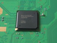
<div style="float:right" | <div style="float:right">[[File:CXD9963GB-PS3slim.jpg|200px|thumb|left|CXD9963GB (SouthBridge)]]</div> | ||
*Used on: | *Used on PS3 models: | ||
** | **[[CECH-20xx]] with motherboard [[DYN-001]] | ||
** | **[[CECH-21xx]] with motherboard [[SUR-001]] | ||
** | **[[CECH-25xx]] with motherboard [[JTP-001]] or [[JSD-001]] | ||
** | **[[CECH-30xx]] with motherboard [[KTE-001]] | ||
** | **[[CECH-40xx]] with motherboard [[MSX-001]] <!-- and PPX-001 PQX-001 --> | ||
** | **[[CECH-43xx]] with motherboard [[REX-001]] <!-- and RTX-001 ---> | ||
As these [[Motherboard Revisions | As these [[Motherboard Revisions | motherboards]] do not have an [[USB]] hub chip, the two frontports are directly connected to this [[South Bridge]] | ||
=== Gallery === | |||
<gallery> | |||
File:CXD9963GB.jpg|CXD9963GB (SouthBridge) | |||
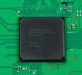
File:CXD9963GB-desoldered-form-JSD001.jpg|CXD9963GB (Desoldered) | |||
File:REX-001 South Bridge pad layout.jpg|REX-001 South Bridge pad layout | |||
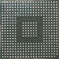
File:CXD9963GB Bottom.jpg|CXD9963GB Bottom | |||
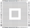
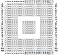
File:CXD9963GB-SB-GRID-bw-chipview.png|CXD9963GB, padlayout<br>SB chip view facing BGA<br>A1 marker:northeast/topright | |||
File:CXD9963GB-SB-GRID-bw-pcbview.png|CXD9963GB, padlayout<br>PCB view facing BGA<br>A1 marker:northwest/topleft | |||
</gallery> | |||
== Pinout == | == Pinout == | ||
{{Motherboard Components}}<noinclude>[[Category:Main]]</noinclude> | {{Motherboard Components}}<noinclude>[[Category:Main]]</noinclude> | ||
Revision as of 13:16, 19 November 2022
CXD9963GB
- Used on PS3 models:
As these motherboards do not have an USB hub chip, the two frontports are directly connected to this South Bridge
Gallery
Pinout
| |||||||||||||||||||||||||||||||||||||||||||||||||||||||||||||||||||||||||||||||||||||||||||||||||||||||||||||||||||||||||||||||||||||||||||||||||||||||||||||||||||||||||||||
