CXM4024R: Difference between revisions
Jump to navigation
Jump to search
mNo edit summary |
No edit summary |
||
| (28 intermediate revisions by 3 users not shown) | |||
| Line 1: | Line 1: | ||
== SCEI CXM4024R | == SCEI CXM4024R (MultiAV Driver) == | ||
<gallery> | |||
File:SCEI_CXM4024R.JPG|SCEI CXM4024R | |||
File:DEH-FH1500J-A - VERTIGO-02 - MultiAV chip.jpg|[[DEH-FH1500J-A]] [[VERTIGO-02]] [[MultiAV]] chip | |||
File:CXM4024R Top.jpg|CXM4024R - Top | |||
CXM4024R Bottom.jpg|CXM4024R - Bottom | |||
</gallery> | |||
Multi chip package, contains CXD3312 and CXA3683<br> | |||
8-753-248-24 / IC2406 <br /> | 8-753-248-24 / IC2406 <br /> | ||
100 tqfp<br /> | 100 tqfp<br /> | ||
Seen on all the PS3 FAT, [[CECHAxx]]/[[COK-00x]] up to including [[CECHQxx]]/[[VER-00x]] | Seen on all the PS3 FAT, [[CECHAxx]]/[[COK-00x]] up to including [[CECHQxx]]/[[VER-00x]] | ||
<div style="float:right">[[File:100pin-TQFP.jpg|200px|thumb|left|100pin-TQFP]]</div> | |||
<div style="float:right">[[File:100pin-TQFP.jpg|200px|thumb|left|100pin-TQFP]]< | {|class="wikitable mw-datatable" style="width:100%; line-height:120%; font-size:90%" | ||
|+ Digital Video Encoder pinout 100 pins | |||
{| | ! style="width:0px; padding:0px" | Pin !! style="width:170px" | Name !! Description | ||
| | |- | ||
| 1 || {{cellcolors|#333|#fff}} AVS || | |||
|- | |||
| 2 || {{cellcolors|#f83|#fff}} VREF2 || Connected to +3.3V_ANA through 2.4K resitor | |||
|- | |- | ||
| | | 3 || {{cellcolors|#333|#fff}} TESTIN || | ||
|- | |- | ||
| | | 4 || {{cellcolors|#333|#fff}} TESTSEL || | ||
|- | |- | ||
| | | 5 || {{cellcolors|#8f8}} BO || Connected to [[MultiAV]] [[Connectors#AV_Multi_Out_pinout_-_CN2401_12P|connector]] pin 4 (Cb/Pb/Blue) through 750ohm resistor ? | ||
|- | |- | ||
| | | 6 || {{cellcolors|#333|#fff}} AGND2 || | ||
|- | |- | ||
| | | 7 || {{cellcolors|#8f8}} GO || Connected to [[MultiAV]] [[Connectors#AV_Multi_Out_pinout_-_CN2401_12P|connector]] pin 1 (Y/Green) through 750ohm resistor ? | ||
|- | |- | ||
| | | 8 || {{cellcolors|#333|#fff}} GND_RGB || | ||
|- | |- | ||
| | | 9 || {{cellcolors|#8f8}} RO || Connected to [[MultiAV]] [[Connectors#AV_Multi_Out_pinout_-_CN2401_12P|connector]] pin 2 (Cr/Pr/Red) through 750ohm resistor ? | ||
|- | |- | ||
| | | 10 || {{cellcolors|#f66|#fff}} AVCC2 / +5V_ANA || | ||
|- | |- | ||
| | | 11 || {{cellcolors|#8f8}} CVBSO || Connected to [[MultiAV]] [[Connectors#AV_Multi_Out_pinout_-_CN2401_12P|connector]] pin 7 (CVIDEO/SYNC) through 750ohm resistor ? | ||
|- | |- | ||
| | | 12 || {{cellcolors|#333|#fff}} GBD_YCCVBS || | ||
|- | |- | ||
| | | 13 || {{cellcolors|#8f8}} CO || Connected to [[MultiAV]] [[Connectors#AV_Multi_Out_pinout_-_CN2401_12P|connector]] pin 6 (C (Y/C)) through 750ohm resistor ? | ||
|- | |- | ||
| | | 14 || {{cellcolors|#333|#fff}} AGND1 || | ||
|- | |- | ||
| | | 15 || {{cellcolors|#8f8}} YO || Connected to [[MultiAV]] [[Connectors#AV_Multi_Out_pinout_-_CN2401_12P|connector]] pin 8 (Y (Y/C)) through 750ohm resistor ? | ||
|- | |- | ||
| | | 16 || {{cellcolors|#f66|#fff}} AVCC1 / +5V_ANA || | ||
|- | |- | ||
| | | 17 || {{cellcolors|#ccc}} S2 || Not Connected | ||
|- | |- | ||
| | | 18 || {{cellcolors|#ccc}} DL3 || Not Connected | ||
|- | |- | ||
| | | 19 || {{cellcolors|#ccc}} DL2 || Not Connected | ||
|- | |- | ||
| | | 20 || {{cellcolors|#ccc}} DL1 || Not Connected | ||
|- | |- | ||
| | | 21 || {{cellcolors|#f33|#fff}} DVD / +1.5V_RSX_VDDIO || | ||
|- | |- | ||
| | | 22 || {{cellcolors|#333|#fff}} VSS || | ||
|- | |- | ||
| | | 23 || {{cellcolors|#f83|#fff}} VG1 || Connected to +3.3V_ANA through 0.1uf capacitor | ||
|- | |- | ||
| | | 24 || {{cellcolors|#f83|#fff}} AVD / +3.3V_ANA || | ||
|- | |- | ||
| | | 25 || {{cellcolors|#333|#fff}} AVS || | ||
|- | |- | ||
! colspan="3" style="padding:1px" data-sort-value="25.5"| | |||
|- | |- | ||
| | | 26 || {{cellcolors|#f83|#fff}} VREF1 || Connected to +3.3V_ANA through 2.4K resitor | ||
|- | |- | ||
| | | 27 || {{cellcolors|#f83|#fff}} AVD / +3.3V_ANA || | ||
|- | |- | ||
| | | 28 || {{cellcolors|#333|#fff}} AVS || | ||
|- | |- | ||
| | | 29 || {{cellcolors|#333|#fff}} VSS || | ||
|- | |- | ||
| | | 30 || {{cellcolors|#333|#fff}} EXTDAC1 || | ||
|- | |- | ||
| | | 31 || {{cellcolors|#6666ff|#ffff00}} RESET || <strike>VO_RST1 ? / Connected to [[RSX]] pad AK38 ([[Template:RSX pad layout 41x41|RSX layout 41x41]]) ?</strike> or<br>Connected to [[Syscon Hardware|Syscon]] pad B5 ([[Template:Syscon_pinout_BGA_200_pads|BGA 200 pads layout]]) | ||
|- | |- | ||
| | | 32 || {{cellcolors|#f6f}} NTPAL || <strike>NT_PL00 ? / Connected to [[RSX]] pad AU33 ([[Template:RSX pad layout 41x41|RSX layout 41x41]]) ?</strike> or<br>NT_PL01 ? / Connected to [[RSX]] pad AA37 ([[Template:RSX pad layout 41x41|RSX layout 41x41]]) ? | ||
|- | |- | ||
| | | 33 || {{cellcolors|#333|#fff}} VSS || | ||
|- | |- | ||
| | | 34 || {{cellcolors|#f6f}} FLD0 || <strike>FLDO0 ? / Connected to [[RSX]] pad AW22 ([[Template:RSX pad layout 41x41|RSX layout 41x41]]) ?</strike> or<br>FLDO1 ? / Connected to [[RSX]] pad AM40 ([[Template:RSX pad layout 41x41|RSX layout 41x41]]) ? | ||
|- | |- | ||
| | | 35 || {{cellcolors|#6666ff|#ffff00}} SCL / DVE_I2C_SCL || Connected to [[Syscon Hardware|Syscon]] pad A10 ([[Template:Syscon_pinout_BGA_200_pads|BGA 200 pads layout]]), or pin 121 ([[Template:Syscon_pinout_LQFP_128_pins|LQFP 128 pins layout]]) | ||
|- | |- | ||
| | | 36 || {{cellcolors|#6666ff|#ffff00}} SDA / DVE_I2C_SDA || Connected to [[Syscon Hardware|Syscon]] pad B10 ([[Template:Syscon_pinout_BGA_200_pads|BGA 200 pads layout]]), or pin 122 ([[Template:Syscon_pinout_LQFP_128_pins|LQFP 128 pins layout]]) | ||
|- | |- | ||
| | | 37 || {{cellcolors|#ff6}} R11 / RSX_VO71 || Connected to [[RSX]] pad AA39 ([[Template:RSX pad layout 41x41|RSX layout 41x41]]) | ||
|- | |- | ||
| | | 38 || {{cellcolors|#ff6}} R10 / RSX_VO70 || Connected to [[RSX]] pad Y35 ([[Template:RSX pad layout 41x41|RSX layout 41x41]]) | ||
|- | |- | ||
| | | 39 || {{cellcolors|#ff6}} R9 / RSX_VO69 || Connected to [[RSX]] pad AA36 ([[Template:RSX pad layout 41x41|RSX layout 41x41]]) | ||
|- | |- | ||
| | | 40 || {{cellcolors|#ff6}} R8 / RSX_VO68 || Connected to [[RSX]] pad AB39 ([[Template:RSX pad layout 41x41|RSX layout 41x41]]) | ||
|- | |- | ||
| | | 41 || {{cellcolors|#ff6}} R7 / RSX_VO67 || Connected to [[RSX]] pad AB36 ([[Template:RSX pad layout 41x41|RSX layout 41x41]]) | ||
|- | |- | ||
| | | 42 || {{cellcolors|#f33|#fff}} DVD / +1.5V_RSX_VDDIO || | ||
|- | |- | ||
| | | 43 || {{cellcolors|#333|#fff}} VSS || | ||
|- | |- | ||
| | | 44 || {{cellcolors|#ff6}} R6 / RSX_VO66 || Connected to [[RSX]] pad AB40 ([[Template:RSX pad layout 41x41|RSX layout 41x41]]) | ||
|- | |- | ||
| | | 45 || {{cellcolors|#ff6}} R5 / RSX_VO65 || Connected to [[RSX]] pad AB38 ([[Template:RSX pad layout 41x41|RSX layout 41x41]]) | ||
|- | |- | ||
| | | 46 || {{cellcolors|#ff6}} R4 / RSX_VO64 || Connected to [[RSX]] pad AB41 ([[Template:RSX pad layout 41x41|RSX layout 41x41]]) | ||
|- | |- | ||
| | | 47 || {{cellcolors|#ff6}} R3 / RSX_VO63 || Connected to [[RSX]] pad AB35 ([[Template:RSX pad layout 41x41|RSX layout 41x41]]) | ||
|- | |- | ||
| | | 48 || {{cellcolors|#ff6}} R2 / RSX_VO62 || Connected to [[RSX]] pad AC40 ([[Template:RSX pad layout 41x41|RSX layout 41x41]]) | ||
|- | |- | ||
| | | 49 || {{cellcolors|#ff6}} R1 / RSX_VO61 || Connected to [[RSX]] pad AD39 ([[Template:RSX pad layout 41x41|RSX layout 41x41]]) | ||
|- | |- | ||
| | | 50 || {{cellcolors|#ff6}} R0 / RSX_VO60 || Connected to [[RSX]] pad AD40 ([[Template:RSX pad layout 41x41|RSX layout 41x41]]) | ||
|- | |- | ||
! colspan="3" style="padding:1px" data-sort-value="50.5"| | |||
|- | |- | ||
| 51 || DVD || | | 51 || {{cellcolors|#f33|#fff}} DVD / +1.5V_RSX_VDDIO || | ||
|- | |- | ||
| 52 || G11 || | | 52 || {{cellcolors|#ff6}} G11 / RSX_VO59 || Connected to [[RSX]] pad AC38 ([[Template:RSX pad layout 41x41|RSX layout 41x41]]) | ||
|- | |- | ||
| 53 || G10 || | | 53 || {{cellcolors|#ff6}} G10 / RSX_VO58 || Connected to [[RSX]] pad AD38 ([[Template:RSX pad layout 41x41|RSX layout 41x41]]) | ||
|- | |- | ||
| 54 || G9 || | | 54 || {{cellcolors|#ff6}} G9 / RSX_VO57 || Connected to [[RSX]] pad AC37 ([[Template:RSX pad layout 41x41|RSX layout 41x41]]) | ||
|- | |- | ||
| 55 || G8 || | | 55 || {{cellcolors|#ff6}} G8 / RSX_VO56 || Connected to [[RSX]] pad AC36 ([[Template:RSX pad layout 41x41|RSX layout 41x41]]) | ||
|- | |- | ||
| 56 || VSS || | | 56 || {{cellcolors|#333|#fff}} VSS || | ||
|- | |- | ||
| 57 || G7 || | | 57 || {{cellcolors|#ff6}} G7 / RSX_VO55 || Connected to [[RSX]] pad AF39 ([[Template:RSX pad layout 41x41|RSX layout 41x41]]) | ||
|- | |- | ||
| 58 || G6 || | | 58 || {{cellcolors|#ff6}} G6 / RSX_VO54 || Connected to [[RSX]] pad AE37 ([[Template:RSX pad layout 41x41|RSX layout 41x41]]) | ||
|- | |- | ||
| 59 || G5 || | | 59 || {{cellcolors|#ff6}} G5 / RSX_VO53 || Connected to [[RSX]] pad AF39 ([[Template:RSX pad layout 41x41|RSX layout 41x41]]) | ||
|- | |- | ||
| 60 || DVD || | | 60 || {{cellcolors|#f33|#fff}} DVD / +1.5V_RSX_VDDIO || | ||
|- | |- | ||
| 61 || G4 || | | 61 || {{cellcolors|#ff6}} G4 / RSX_VO52 || Connected to [[RSX]] pad AD35 ([[Template:RSX pad layout 41x41|RSX layout 41x41]]) | ||
|- | |- | ||
| 62 || G3 || | | 62 || {{cellcolors|#ff6}} G3 / RSX_VO51 || Connected to [[RSX]] pad AF40 ([[Template:RSX pad layout 41x41|RSX layout 41x41]]) | ||
|- | |- | ||
| 63 || G2 || | | 63 || {{cellcolors|#ff6}} G2 / RSX_VO50 || Connected to [[RSX]] pad AF36 ([[Template:RSX pad layout 41x41|RSX layout 41x41]]) | ||
|- | |- | ||
| 64 || G1 || | | 64 || {{cellcolors|#ff6}} G1 / RSX_VO49 || Connected to [[RSX]] pad AG40 ([[Template:RSX pad layout 41x41|RSX layout 41x41]]) | ||
|- | |- | ||
| 65 || G0 || | | 65 || {{cellcolors|#ff6}} G0 / RSX_VO48 || Connected to [[RSX]] pad AF38 ([[Template:RSX pad layout 41x41|RSX layout 41x41]]) | ||
|- | |- | ||
| 66 || B11 || | | 66 || {{cellcolors|#ff6}} B11 / RSX_VO47 || Connected to [[RSX]] pad AF35 ([[Template:RSX pad layout 41x41|RSX layout 41x41]]) | ||
|- | |- | ||
| 67 || B10 || | | 67 || {{cellcolors|#ff6}} B10 / RSX_VO46 || Connected to [[RSX]] pad AH39 ([[Template:RSX pad layout 41x41|RSX layout 41x41]]) | ||
|- | |- | ||
| 68 || B9 || | | 68 || {{cellcolors|#ff6}} B9 / RSX_VO45 || Connected to [[RSX]] pad AG38 ([[Template:RSX pad layout 41x41|RSX layout 41x41]]) | ||
|- | |- | ||
| 69 || B8 || | | 69 || {{cellcolors|#ff6}} B8 / RSX_VO44 || Connected to [[RSX]] pad AH40 ([[Template:RSX pad layout 41x41|RSX layout 41x41]]) | ||
|- | |- | ||
| 70 || DVD || | | 70 || {{cellcolors|#f33|#fff}} DVD / +1.5V_RSX_VDDIO || | ||
|- | |- | ||
| 71 || VSS || | | 71 || {{cellcolors|#333|#fff}} VSS || | ||
|- | |- | ||
| 72 || B7 || | | 72 || {{cellcolors|#ff6}} B7 / RSX_VO43 || Connected to [[RSX]] pad AG37 ([[Template:RSX pad layout 41x41|RSX layout 41x41]]) | ||
|- | |- | ||
| 73 || B6 || | | 73 || {{cellcolors|#ff6}} B6 / RSX_VO42 || Connected to [[RSX]] pad AH38 ([[Template:RSX pad layout 41x41|RSX layout 41x41]]) | ||
|- | |- | ||
| 74 || B5 || | | 74 || {{cellcolors|#ff6}} B5 / RSX_VO41 || Connected to [[RSX]] pad AG36 ([[Template:RSX pad layout 41x41|RSX layout 41x41]]) | ||
|- | |- | ||
| 75 || B4 || | | 75 || {{cellcolors|#ff6}} B4 / RSX_VO40 || Connected to [[RSX]] pad AJ39 ([[Template:RSX pad layout 41x41|RSX layout 41x41]]) | ||
|- | |- | ||
! colspan="3" style="padding:1px" data-sort-value="75.5"| | |||
|- | |- | ||
| | | 76 || {{cellcolors|#ff6}} B3 / RSX_VO39 || Connected to [[RSX]] pad AK39 ([[Template:RSX pad layout 41x41|RSX layout 41x41]]) | ||
|- | |- | ||
| | | 77 || {{cellcolors|#ff6}} B2 / RSX_VO38 || Connected to [[RSX]] pad AK41 ([[Template:RSX pad layout 41x41|RSX layout 41x41]]) | ||
|- | |- | ||
| | | 78 || {{cellcolors|#ff6}} B1 / RSX_VO37 || Connected to [[RSX]] pad AJ37 ([[Template:RSX pad layout 41x41|RSX layout 41x41]]) | ||
|- | |- | ||
| | | 79 || {{cellcolors|#ff6}} B0 / RSX_VO36 || Connected to [[RSX]] pad AH35 ([[Template:RSX pad layout 41x41|RSX layout 41x41]]) | ||
|- | |- | ||
| | | 80 || {{cellcolors|#f6f}} CSYNC || CSYNC_01 ? / Connected to [[RSX]] pad AJ36 ([[Template:RSX pad layout 41x41|RSX layout 41x41]]) ? | ||
|- | |- | ||
| | | 81 || {{cellcolors|#f33|#fff}} DVD / +1.5V_RSX_VDDIO || | ||
|- | |- | ||
| | | 82 || {{cellcolors|#333|#fff}} VSS || | ||
|- | |- | ||
| | | 83 || {{cellcolors|#f6f}} VSYNC || VSYNC_01 ? / Connected to [[RSX]] pad AK36 ([[Template:RSX pad layout 41x41|RSX layout 41x41]]) ? | ||
|- | |- | ||
| | | 84 || {{cellcolors|#f6f}} HSYNC || HSYNC_01 ? / Connected to [[RSX]] pad AK40 ([[Template:RSX pad layout 41x41|RSX layout 41x41]]) ? | ||
|- | |- | ||
| | | 85 || {{cellcolors|#f6f}} DEN || RSX_VO_DE1 ? / Connected to [[RSX]] pad AL40 ([[Template:RSX pad layout 41x41|RSX layout 41x41]]) ? | ||
|- | |- | ||
| | | 86 || {{cellcolors|#333|#fff}} TMODE1 || | ||
|- | |- | ||
| | | 87 || {{cellcolors|#333|#fff}} TMODE0 || | ||
|- | |- | ||
| | | 88 || {{cellcolors|#f33|#fff}} DVD / +1.5V_RSX_VDDIO || | ||
|- | |- | ||
| | | 89 || {{cellcolors|#ccc}} HSYNC0 || Not Connected | ||
|- | |- | ||
| | | 90 || {{cellcolors|#ccc}} VSYNCO || Not Connected | ||
|- | |- | ||
| | | 91 || {{cellcolors|#ccc}} PLLOUT || Not Connected | ||
|- | |- | ||
| | | 92 || {{cellcolors|#333|#fff}} SCAN_ENABLE || | ||
|- | |- | ||
| | | 93 || {{cellcolors|#f6f}} CLOCK || RSX_CLKOUT1 ? / Connected to [[RSX]] pad AE36 ([[Template:RSX pad layout 41x41|RSX layout 41x41]]) ? | ||
|- | |- | ||
| | | 94 || {{cellcolors|#333|#fff}} VSS || | ||
|- | |- | ||
| | | 95 || {{cellcolors|#333|#fff}} VSSP || | ||
|- | |- | ||
| | | 96 || {{cellcolors|#f33|#fff}} DVDP / +1.5V_RSX_VDDIO || | ||
|- | |- | ||
| | | 97 || {{cellcolors|#333|#fff}} AVS || | ||
|- | |- | ||
| | | 98 || {{cellcolors|#f83|#fff}} AVD / +3.3V_ANA || | ||
|- | |- | ||
| | | 99 || {{cellcolors|#f83|#fff}} VG2 || Connected to +3.3V_ANA through 0.1uf capacitor | ||
|- | |- | ||
| 100 || {{cellcolors|#f83|#fff}} AVD / +3.3V_ANA || | |||
|} | |} | ||
{{Motherboard Components}}<noinclude>[[Category:Main]]</noinclude> | {{Motherboard Components}}<noinclude>[[Category:Main]]</noinclude> | ||
Latest revision as of 07:52, 19 October 2022
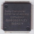
SCEI CXM4024R (MultiAV Driver)[edit | edit source]
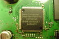
SCEI CXM4024R
CXM4024R - Top
CXM4024R - Bottom


Multi chip package, contains CXD3312 and CXA3683
8-753-248-24 / IC2406
100 tqfp
Seen on all the PS3 FAT, CECHAxx/COK-00x up to including CECHQxx/VER-00x

| Pin | Name | Description |
|---|---|---|
| 1 | AVS | |
| 2 | VREF2 | Connected to +3.3V_ANA through 2.4K resitor |
| 3 | TESTIN | |
| 4 | TESTSEL | |
| 5 | BO | Connected to MultiAV connector pin 4 (Cb/Pb/Blue) through 750ohm resistor ? |
| 6 | AGND2 | |
| 7 | GO | Connected to MultiAV connector pin 1 (Y/Green) through 750ohm resistor ? |
| 8 | GND_RGB | |
| 9 | RO | Connected to MultiAV connector pin 2 (Cr/Pr/Red) through 750ohm resistor ? |
| 10 | AVCC2 / +5V_ANA | |
| 11 | CVBSO | Connected to MultiAV connector pin 7 (CVIDEO/SYNC) through 750ohm resistor ? |
| 12 | GBD_YCCVBS | |
| 13 | CO | Connected to MultiAV connector pin 6 (C (Y/C)) through 750ohm resistor ? |
| 14 | AGND1 | |
| 15 | YO | Connected to MultiAV connector pin 8 (Y (Y/C)) through 750ohm resistor ? |
| 16 | AVCC1 / +5V_ANA | |
| 17 | S2 | Not Connected |
| 18 | DL3 | Not Connected |
| 19 | DL2 | Not Connected |
| 20 | DL1 | Not Connected |
| 21 | DVD / +1.5V_RSX_VDDIO | |
| 22 | VSS | |
| 23 | VG1 | Connected to +3.3V_ANA through 0.1uf capacitor |
| 24 | AVD / +3.3V_ANA | |
| 25 | AVS | |
| 26 | VREF1 | Connected to +3.3V_ANA through 2.4K resitor |
| 27 | AVD / +3.3V_ANA | |
| 28 | AVS | |
| 29 | VSS | |
| 30 | EXTDAC1 | |
| 31 | RESET | Connected to Syscon pad B5 (BGA 200 pads layout) |
| 32 | NTPAL | NT_PL01 ? / Connected to RSX pad AA37 (RSX layout 41x41) ? |
| 33 | VSS | |
| 34 | FLD0 | FLDO1 ? / Connected to RSX pad AM40 (RSX layout 41x41) ? |
| 35 | SCL / DVE_I2C_SCL | Connected to Syscon pad A10 (BGA 200 pads layout), or pin 121 (LQFP 128 pins layout) |
| 36 | SDA / DVE_I2C_SDA | Connected to Syscon pad B10 (BGA 200 pads layout), or pin 122 (LQFP 128 pins layout) |
| 37 | R11 / RSX_VO71 | Connected to RSX pad AA39 (RSX layout 41x41) |
| 38 | R10 / RSX_VO70 | Connected to RSX pad Y35 (RSX layout 41x41) |
| 39 | R9 / RSX_VO69 | Connected to RSX pad AA36 (RSX layout 41x41) |
| 40 | R8 / RSX_VO68 | Connected to RSX pad AB39 (RSX layout 41x41) |
| 41 | R7 / RSX_VO67 | Connected to RSX pad AB36 (RSX layout 41x41) |
| 42 | DVD / +1.5V_RSX_VDDIO | |
| 43 | VSS | |
| 44 | R6 / RSX_VO66 | Connected to RSX pad AB40 (RSX layout 41x41) |
| 45 | R5 / RSX_VO65 | Connected to RSX pad AB38 (RSX layout 41x41) |
| 46 | R4 / RSX_VO64 | Connected to RSX pad AB41 (RSX layout 41x41) |
| 47 | R3 / RSX_VO63 | Connected to RSX pad AB35 (RSX layout 41x41) |
| 48 | R2 / RSX_VO62 | Connected to RSX pad AC40 (RSX layout 41x41) |
| 49 | R1 / RSX_VO61 | Connected to RSX pad AD39 (RSX layout 41x41) |
| 50 | R0 / RSX_VO60 | Connected to RSX pad AD40 (RSX layout 41x41) |
| 51 | DVD / +1.5V_RSX_VDDIO | |
| 52 | G11 / RSX_VO59 | Connected to RSX pad AC38 (RSX layout 41x41) |
| 53 | G10 / RSX_VO58 | Connected to RSX pad AD38 (RSX layout 41x41) |
| 54 | G9 / RSX_VO57 | Connected to RSX pad AC37 (RSX layout 41x41) |
| 55 | G8 / RSX_VO56 | Connected to RSX pad AC36 (RSX layout 41x41) |
| 56 | VSS | |
| 57 | G7 / RSX_VO55 | Connected to RSX pad AF39 (RSX layout 41x41) |
| 58 | G6 / RSX_VO54 | Connected to RSX pad AE37 (RSX layout 41x41) |
| 59 | G5 / RSX_VO53 | Connected to RSX pad AF39 (RSX layout 41x41) |
| 60 | DVD / +1.5V_RSX_VDDIO | |
| 61 | G4 / RSX_VO52 | Connected to RSX pad AD35 (RSX layout 41x41) |
| 62 | G3 / RSX_VO51 | Connected to RSX pad AF40 (RSX layout 41x41) |
| 63 | G2 / RSX_VO50 | Connected to RSX pad AF36 (RSX layout 41x41) |
| 64 | G1 / RSX_VO49 | Connected to RSX pad AG40 (RSX layout 41x41) |
| 65 | G0 / RSX_VO48 | Connected to RSX pad AF38 (RSX layout 41x41) |
| 66 | B11 / RSX_VO47 | Connected to RSX pad AF35 (RSX layout 41x41) |
| 67 | B10 / RSX_VO46 | Connected to RSX pad AH39 (RSX layout 41x41) |
| 68 | B9 / RSX_VO45 | Connected to RSX pad AG38 (RSX layout 41x41) |
| 69 | B8 / RSX_VO44 | Connected to RSX pad AH40 (RSX layout 41x41) |
| 70 | DVD / +1.5V_RSX_VDDIO | |
| 71 | VSS | |
| 72 | B7 / RSX_VO43 | Connected to RSX pad AG37 (RSX layout 41x41) |
| 73 | B6 / RSX_VO42 | Connected to RSX pad AH38 (RSX layout 41x41) |
| 74 | B5 / RSX_VO41 | Connected to RSX pad AG36 (RSX layout 41x41) |
| 75 | B4 / RSX_VO40 | Connected to RSX pad AJ39 (RSX layout 41x41) |
| 76 | B3 / RSX_VO39 | Connected to RSX pad AK39 (RSX layout 41x41) |
| 77 | B2 / RSX_VO38 | Connected to RSX pad AK41 (RSX layout 41x41) |
| 78 | B1 / RSX_VO37 | Connected to RSX pad AJ37 (RSX layout 41x41) |
| 79 | B0 / RSX_VO36 | Connected to RSX pad AH35 (RSX layout 41x41) |
| 80 | CSYNC | CSYNC_01 ? / Connected to RSX pad AJ36 (RSX layout 41x41) ? |
| 81 | DVD / +1.5V_RSX_VDDIO | |
| 82 | VSS | |
| 83 | VSYNC | VSYNC_01 ? / Connected to RSX pad AK36 (RSX layout 41x41) ? |
| 84 | HSYNC | HSYNC_01 ? / Connected to RSX pad AK40 (RSX layout 41x41) ? |
| 85 | DEN | RSX_VO_DE1 ? / Connected to RSX pad AL40 (RSX layout 41x41) ? |
| 86 | TMODE1 | |
| 87 | TMODE0 | |
| 88 | DVD / +1.5V_RSX_VDDIO | |
| 89 | HSYNC0 | Not Connected |
| 90 | VSYNCO | Not Connected |
| 91 | PLLOUT | Not Connected |
| 92 | SCAN_ENABLE | |
| 93 | CLOCK | RSX_CLKOUT1 ? / Connected to RSX pad AE36 (RSX layout 41x41) ? |
| 94 | VSS | |
| 95 | VSSP | |
| 96 | DVDP / +1.5V_RSX_VDDIO | |
| 97 | AVS | |
| 98 | AVD / +3.3V_ANA | |
| 99 | VG2 | Connected to +3.3V_ANA through 0.1uf capacitor |
| 100 | AVD / +3.3V_ANA | |
| |||||||||||||||||||||||||||||||||||||||||||||||||||||||||||||||||||||||||||||||||||||||||||||||||||||||||||||||||||||||||||||||||||||||||||||||||||||||||||||||||||||||||||||
