CXR713120-201GB: Difference between revisions
Jump to navigation
Jump to search
m (→Pinout: Problems in the pad names "SEL2_I2C_SCL" and "SEL2_I2C_SDA". The same names are repeated 2 times each, we need to give them a unique name) |
m (Moved to Template:Syscon Pinout BGA 200 pads) |
||
| Line 1: | Line 1: | ||
== Generation 1: CXR713120-201GB / CXR713120-201GB-TL (SysCon) == | == Generation 1: CXR713120-201GB / CXR713120-201GB-TL (SysCon) == | ||
<div style="float:right" | <div style="float:right">[[File:SYSCON_GEN1.JPG|thumb|Syscon [[CXR713120-201GB]]]]</div> | ||
8-753-279-04 / IC4002 <br /> | 8-753-279-04 / IC4002 <br /> | ||
Early PS3 : up to including [[CECHKxx]]/[[DIA-00x#DIA-002|DIA-002]] | Early PS3 : up to including [[CECHKxx]]/[[DIA-00x#DIA-002|DIA-002]] | ||
<br style="clear: both;" /> | |||
=== Pinout === | === Pinout === | ||
{ | {{Syscon Pinout BGA 200 pads}} | ||
=== Intercepting signals === | === Intercepting signals === | ||
Revision as of 17:35, 29 May 2021
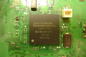
Generation 1: CXR713120-201GB / CXR713120-201GB-TL (SysCon)

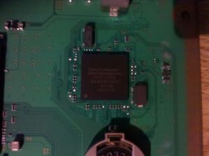
Syscon CXR713120-201GB
8-753-279-04 / IC4002
Early PS3 : up to including CECHKxx/DIA-002
Pinout
Template:Syscon Pinout BGA 200 pads
Intercepting signals
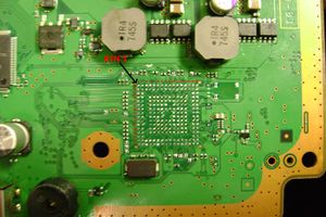
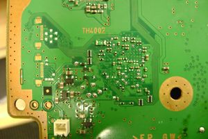
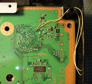
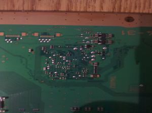
This points are availables to intercept signals by soldering wires, attaching probes, osciloscopes, etc... The photos are only orientatives to follow the traces, there's no need to remove the SYSCON to intercept this signals so can be done while its working
All this points has been hardware reverse engineered from a CECHH02/DIA-001 motherboard
Topside Pinout
| Pin # | Name | Description |
|---|---|---|
| B3 | SW_10 | Unknown |
| A6 | MC_RESERVED2 | Unknown |
| E10 | MUL_CHKSTP_OUT | Unknown |
| C15 | VSS | Power Ground |
| B16 | OSCOUT | Goes to unpopulated crystal |
| C16 | OSCIN | From unpupulated crystal |
| B15 | POW_FAIL | Power Failure Signal |
| H1 | PN5 | Unknown |
| H2 | PN6 | Unknown |
| R1 | PM7 | Unknown |
| R2 | PM6 | Unknown |
| M4 | SW9 | Unknown |
| M10 | XDR_FET_SCK | Unknown |
Bottomside Pinout
| Pin # | Name | Description |
|---|---|---|
| R5 | VDD | +3.3v |
| R7 | DVDD | +1.8v |
| C15 | VSS | Power Ground |
| N16 | DIAG_MODE | Unknown |
| N15 | BACKUP_MODE | Unknown |
| P16 | UART0_TxD | Serial |
| P15 | UART0_RxD | Serial |
| R9 | PQ1 | Unknown |
| B12 | POW_SW | Power Switch |
| A12 | EJECT_SW | Eject Switch |
| L7 | JNTAST | JTAG |
| L8 | JRTCK | JTAG |
| L9 | JTMS | JTAG |
| K7 | JTDI | JTAG |
| K8 | JTCK | JTAG |
| K9 | JTDO | JTAG |
| M6 | SW_7_B | Unknown |
| M8 | FANPWM1 | Unknown |
| E5 | GX_VSRT | Unknown |
| B5 | DVE_RST | Unknown |
| G4 | HDMI_RST1 | Unknown |
| D4 | XDR_FET_RST | Unknown |
Perimeter traces
CECHG01 Pictures - SEM-001
Topside Pictures
Bottomside Pictures
| |||||||||||||||||||||||||||||||||||||||||||||||||||||||||||||||||||||||||||||||||||||||||||||||||||||||||||||||||||||||||||||||||||||||||||||||||||||||||||||||||||||||||||||
