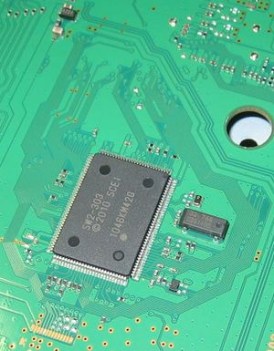
SW2-303: Difference between revisions
Jump to navigation
Jump to search
m (→Pinout: this note was verifyed wrong... what happened is the info posted for pins 12 and 13 was "displaced" (mistake at counting pins)... but did belong to pins 11 and 12 instead) |
m (→Pinout) |
||
| Line 20: | Line 20: | ||
| 6 || P36/STBY_LED || || Connected to dual led(Red) on switchboard through the dual digital NPN trans. EMH1(SOT-563). 3v @ standby (3.3V) || 3.3 | | 6 || P36/STBY_LED || || Connected to dual led(Red) on switchboard through the dual digital NPN trans. EMH1(SOT-563). 3v @ standby (3.3V) || 3.3 | ||
|- | |- | ||
| 7 || || || || 0 | | 7 || || || Connected to pinAA18@SB || 0 | ||
|- | |- | ||
| 8 || || || || 0 | | 8 || || || || 0 | ||
Revision as of 19:46, 12 September 2018
SW2-303 (SysCon)
First to be seen on PS3 Slim CECH-25xx with motherboards: JSD-00x/JTP-00x
Pinout
| Pin # | Name | Port | Description | STBY Voltages |
|---|---|---|---|---|
| 1 | Connected to pin27 @Panasonic MN8647091 | 0 | ||
| 2 | P141 | Connected to pinD1@SB through the resistor. ~1V @ standby (0 V?) | 0 | |
| 3 | P140 | pinBA17@BE connected through the NPN transistor. 3V @ standby (3.15V) | 3.15 | |
| 4 | To +12V_MAIN through the resistor and divider | 0 | ||
| 5 | P37/POW_LED | Connected to dual led(Green) on switchboard through the dual digital NPN trans. EMH1(SOT-563) | 0 | |
| 6 | P36/STBY_LED | Connected to dual led(Red) on switchboard through the dual digital NPN trans. EMH1(SOT-563). 3v @ standby (3.3V) | 3.3 | |
| 7 | Connected to pinAA18@SB | 0 | ||
| 8 | 0 | |||
| 9 | 0 | |||
| 10 | 0 | |||
| 11 | P106 | Connected to Backlit LEDs @SWITCH Board | 0 | |
| 12 | P105 | Connected to CONTOUR LEDs @SWITCH Board | 0 | |
| 13 | P104 | 0 | ||
| 14 | 0 | |||
| 15 | 0 | |||
| 16 | BUZZER | 0 | ||
| 17 | 0 | |||
| 18 | P44 | 3v @ standby | 3.0 | |
| 19 | 0 | |||
| 20 | 0 | |||
| 21 | P41 | 3v @ standby | 3.0 | |
| 22 | TOOL0/Debugger Pin? | (Connected to Pin 7 @ Service Connector) (0V?) | 0 | |
| 23 | 0 | |||
| 24 | P126/THR_I2C_SDA | Connected to pin 7 of CELL/RSX temperature monitor IC's (SMbus I2C shared data line) | 3v @ standby (3.15) | |
| 25 | P125/THR_I2C_SCL | Connected to pin 8 of CELL/RSX temperature monitor IC's (SMbus I2C shared clock line) | 3v @ standby (3.15) | |
| 26 | RESET? | Connected to standby voltage regulator 463A, pin 3 | ||
| 27 | P124 | CLK -> 1-2V Amplitude (32.768Khz?) | ||
| 28 | P123 | CLK -> 1-2V Amplitude (32.768Khz?) | ||
| 29 | P137/FLMD0 | 3.3v @ standby (Connected to pin 8 at Service Connector through the resistor) | 3.33 | |
| 30 | P122 | 0.8v @ standby | 1.1 | |
| 31 | P121 | 2.2v @ standby | 2.4 | |
| 32 | REGC | |||
| 33 | GROUND/Vss0 | 0 | ||
| 34 | GROUND/EVss0 | 0 | ||
| 35 | Vdd | Connected to voltage regulator 463A, pin 2 (3.3_EVER_B) | 3v @ standby (3.3) | |
| 36 | EVdd0 | Connected to voltage regulator 463A, pin 2 (3.3_EVER_B) | 3v @ standby (3.3) | |
| 37 | P60 | 0.2v @ standby | 0 | |
| 38 | P61 | 0.2v @ standby | 0 | |
| 39 | 0 | |||
| 40 | 0 | |||
| 41 | P31/AC IN? | 3v @ standby (3.3) | 3.3 | |
| 42 | Connected (indirectly) to voltage regulator BD9684 0906, pin 4 | 0 | ||
| 43 | P65 | 3v @ standby | 3.0 | |
| 44 | 0 | |||
| 45 | 0 | |||
| 46 | 0 | |||
| 47 | P76 | 3v @ standby (3.15) | 3.15 | |
| 48 | P75 | 3v @ standby (3.15) | 3.15 | |
| 49 | 0 | |||
| 50 | P73 | Connected to voltage regulator D35653 0S25, pin 5 (And connected to pin 3 @ Service Connector) | 0 | |
| 51 | 0 | |||
| 52 | Connected to voltage regulator BD3525, pin 12 | 0 | ||
| 53 | 0 | |||
| 54 | 0 | |||
| 55 | 0 | |||
| 56 | GROUND/EVss1 | 0 | ||
| 57 | EVdd1 | Connected to voltage regulator 463A, pin 2 (3.3_EVER_B) | 3v @ standby (3.3) | |
| 58 | 0 | |||
| 59 | 0 | |||
| 60 | 0 | |||
| 61 | 0 | |||
| 62 | 0 | |||
| 63 | 0 | |||
| 64 | 0 | |||
| 65 | 0 | |||
| 66 | 0 | |||
| 67 | 0 | |||
| 68 | 0 | |||
| 69 | 0 | |||
| 70 | 0 | |||
| 71 | 0 | |||
| 72 | 0 | |||
| 73 | 0 | |||
| 74 | 0 | |||
| 75 | Connected to voltage regulator Mitsumi 040 810X, pin 5 | 0 | ||
| 76 | P16 | 3v @ standby (3.15) | 3.15 | |
| 77 | P15 | 3v @ standby (3.3) | 3.3 | |
| 78 | SC_RxD(RxD3/RxD2/P14) | 0 | ||
| 79 | SC_TxD(TxD3/TxD2/P13) | 3v @ standby (3.3) | 3.3 | |
| 80 | 0 | |||
| 81 | P11 | 1v @ standby | 0 | |
| 82 | 0 | |||
| 83 | P90 | 2v @ standby | 0 | |
| 84 | P91 | 3v @ standby | 3.0 | |
| 85 | 0 | |||
| 86 | 0 | |||
| 87 | 0 | |||
| 88 | 0 | |||
| 89 | 0 | |||
| 90 | 0 | |||
| 91 | 0 | |||
| 92 | Connected to voltage regulator BD3527 (near FLASH), pin 12 | 0 | ||
| 93 | 0 | |||
| 94 | 0 | |||
| 95 | Connected to voltage regulator BD3527 (near USB), pin 12 | 0 | ||
| 96 | 0 | |||
| 97 | P101 | Connected to voltage regulator 463A, pin 2 (3.3_EVER_B) | 3v @ standby (3.3) | |
| 98 | 0 | |||
| 99 | 0 | |||
| 100 | P146 | Connected to voltage regulator 463A, pin 2 (3.3_EVER_B) | 3v @ standby (3.3) | |
| 101 | GROUND | 0 | ||
| 102 | 0 | |||
| 103 | 0 | |||
| 104 | 0 | |||
| 105 | 0 | |||
| 106 | 0 | |||
| 107 | 0 | |||
| 108 | 0 | |||
| 109 | P150 | 3v @ standby | 3.0 | |
| 110 | P27/POW_SW | 3v @ standby (3.3) | 3.3 | |
| 111 | P26/EJECT_SW | 3v @ standby (3.3) | 3.3 | |
| 112 | 0 | |||
| 113 | 0 | |||
| 114 | 0 | |||
| 115 | 0 | |||
| 116 | 0 | |||
| 117 | P20 | (0V?) | 0 | |
| 118 | P130/ACDC_STBY | 0 | ||
| 119 | P102 | Connected to standby voltage regulator 348A, pins 2 and 7 | ||
| 120 | 0 | |||
| 121 | 0 | |||
| 122 | 0 | |||
| 123 | 0 | |||
| 124 | Connected to pin93 @Panasonic MN8647091 | 0 | ||
| 125 | 0 | |||
| 126 | P145/FAN_PWM | PWM Control for the Fan. | 0 | |
| 127 | 0 | |||
| 128 | Connected to pin29 @Panasonic MN8647091 | 0 |
| This article is marked for rewrite/restructuring in proper wiki format. You can help PS3 Developer wiki by editing it. |
| |||||||||||||||||||||||||||||||||||||||||||||||||||||||||||||||||||||||||||||||||||||||||||||||||||||||||||||||||||||||||||||||||||||||||||||||||||||||||||||||||||||||||||||


