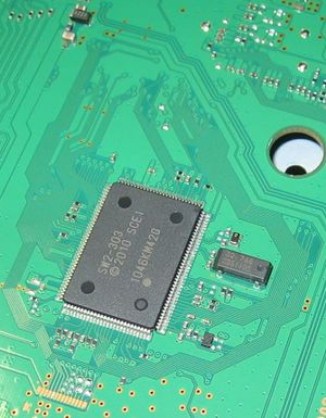
SW2-303: Difference between revisions
Jump to navigation
Jump to search
m (→Pinout) |
|||
| Line 24: | Line 24: | ||
| 8 || || || Connected to pinAA17@SB || 0 | | 8 || || || Connected to pinAA17@SB || 0 | ||
|- | |- | ||
| 9 || || || || 0 | | 9 || || || CELL BE related? || 0 | ||
|- | |- | ||
| 10 || || || || 0 | | 10 || || || || 0 | ||
Revision as of 22:54, 12 September 2018
SW2-303 (SysCon)
First to be seen on PS3 Slim CECH-25xx with motherboards: JSD-00x/JTP-00x
Pinout
| Pin # | Name | Port | Description | STBY Voltages |
|---|---|---|---|---|
| 1 | Connected to pin27 @Panasonic MN8647091 | 0 | ||
| 2 | P141 | Connected to pinD1@SB through the resistor. ~1V @ standby (0 V?) | 0 | |
| 3 | P140 | pinBA17@BE connected through the NPN transistor. 3V @ standby (3.15V) | 3.15 | |
| 4 | To +12V_MAIN through the resistor and divider | 0 | ||
| 5 | P37/POW_LED | Connected to dual led(Green) on switch board through the dual digital NPN trans. EMH1(SOT-563) | 0 | |
| 6 | P36/STBY_LED | Connected to dual led(Red) on switch board through the dual digital NPN trans. EMH1(SOT-563) | 3v @ standby (3.3V) | |
| 7 | Connected to pinAA18@SB | 0 | ||
| 8 | Connected to pinAA17@SB | 0 | ||
| 9 | CELL BE related? | 0 | ||
| 10 | 0 | |||
| 11 | P106 | Connected to Backlit LEDs on switch board | 0 | |
| 12 | P105 | Connected to CONTOUR LEDs on switch board | 0 | |
| 13 | P104 | Absent element between this line and GND. Nothing else. | 0 | |
| 14 | 0 | |||
| 15 | 0 | |||
| 16 | BUZZER | 0 | ||
| 17 | 0 | |||
| 18 | P44 | 3v @ standby | 3.0 | |
| 19 | 0 | |||
| 20 | 0 | |||
| 21 | P41 | 3v @ standby | 3.0 | |
| 22 | TOOL0/Debugger Pin? | (Connected to Pin 7 @ Service Connector) (0V?) | 0 | |
| 23 | 0 | |||
| 24 | P126/THR_I2C_SDA | Connected to pin 7 of CELL/RSX temperature monitor IC's (SMbus I2C shared data line) | 3v @ standby (3.15) | |
| 25 | P125/THR_I2C_SCL | Connected to pin 8 of CELL/RSX temperature monitor IC's (SMbus I2C shared clock line) | 3v @ standby (3.15) | |
| 26 | RESET? | Connected to standby voltage regulator 463A, pin 3 | ||
| 27 | P124 | Connected to the big black external oscilator 1 next to syscon. CLK -> 1-2V Amplitude (32.768Khz?) | ||
| 28 | P123 | Connected to the big black external oscilator 1 next to syscon. CLK -> 1-2V Amplitude (32.768Khz?) | ||
| 29 | P137/FLMD0 | 3.3v @ standby (Connected to pin 8 at Service Connector through the resistor) | 3.33 | |
| 30 | P122 | Connected to a small external oscilator 2 ? | 0.8v @ standby (1.1) | |
| 31 | P121 | Connected to a small external oscilator 2 ? | 2.2v @ standby (2.4) | |
| 32 | REGC | |||
| 33 | GROUND/Vss0 | 0 | ||
| 34 | GROUND/EVss0 | 0 | ||
| 35 | Vdd | Connected to voltage regulator 463A, pin 2 (3.3_EVER_B) | 3v @ standby (3.3) | |
| 36 | EVdd0 | Connected to voltage regulator 463A, pin 2 (3.3_EVER_B) | 3v @ standby (3.3) | |
| 37 | P60 | 0.2v @ standby | 0 | |
| 38 | P61 | 0.2v @ standby | 0 | |
| 39 | 0 | |||
| 40 | 0 | |||
| 41 | P31/AC IN? | 3v @ standby (3.3) | 3.3 | |
| 42 | Connected (indirectly) to voltage regulator BD9684 0906, pin 4 | 0 | ||
| 43 | P65 | 3v @ standby | 3.0 | |
| 44 | 0 | |||
| 45 | 0 | |||
| 46 | 0 | |||
| 47 | P76 | 3v @ standby (3.15) | 3.15 | |
| 48 | P75 | 3v @ standby (3.15) | 3.15 | |
| 49 | 0 | |||
| 50 | P73 | Connected to voltage regulator D35653 0S25, pin 5 (And connected to pin 3 @ Service Connector) | 0 | |
| 51 | 0 | |||
| 52 | Connected to voltage regulator BD3525, pin 12 | 0 | ||
| 53 | 0 | |||
| 54 | 0 | |||
| 55 | 0 | |||
| 56 | GROUND/EVss1 | 0 | ||
| 57 | EVdd1 | Connected to voltage regulator 463A, pin 2 (3.3_EVER_B) | 3v @ standby (3.3) | |
| 58 | 0 | |||
| 59 | 0 | |||
| 60 | 0 | |||
| 61 | 0 | |||
| 62 | 0 | |||
| 63 | 0 | |||
| 64 | 0 | |||
| 65 | 0 | |||
| 66 | 0 | |||
| 67 | 0 | |||
| 68 | 0 | |||
| 69 | 0 | |||
| 70 | 0 | |||
| 71 | 0 | |||
| 72 | 0 | |||
| 73 | 0 | |||
| 74 | 0 | |||
| 75 | Connected to voltage regulator Mitsumi 040 810X, pin 5 | 0 | ||
| 76 | P16 | 3v @ standby (3.15) | 3.15 | |
| 77 | P15 | 3v @ standby (3.3) | 3.3 | |
| 78 | SC_RxD(RxD3/RxD2/P14) | 0 | ||
| 79 | SC_TxD(TxD3/TxD2/P13) | 3v @ standby (3.3) | 3.3 | |
| 80 | 0 | |||
| 81 | P11 | 1v @ standby | 0 | |
| 82 | 0 | |||
| 83 | P90 | 2v @ standby | 0 | |
| 84 | P91 | 3v @ standby | 3.0 | |
| 85 | 0 | |||
| 86 | 0 | |||
| 87 | 0 | |||
| 88 | 0 | |||
| 89 | 0 | |||
| 90 | 0 | |||
| 91 | 0 | |||
| 92 | Connected to voltage regulator BD3527 (near FLASH), pin 12 | 0 | ||
| 93 | 0 | |||
| 94 | 0 | |||
| 95 | Connected to voltage regulator BD3527 (near USB), pin 12 | 0 | ||
| 96 | 0 | |||
| 97 | P101 | Connected to voltage regulator 463A, pin 2 (3.3_EVER_B) | 3v @ standby (3.3) | |
| 98 | 0 | |||
| 99 | 0 | |||
| 100 | P146 | Connected to voltage regulator 463A, pin 2 (3.3_EVER_B) | 3v @ standby (3.3) | |
| 101 | GROUND | 0 | ||
| 102 | 0 | |||
| 103 | 0 | |||
| 104 | 0 | |||
| 105 | 0 | |||
| 106 | 0 | |||
| 107 | 0 | |||
| 108 | 0 | |||
| 109 | P150 | 3v @ standby | 3.0 | |
| 110 | P27/POW_SW_DET | Power switch detect. Connected to switch board | 3v @ standby (3.3) 3.3 | |
| 111 | P26/EJECT_SW_DET | Eject switch detect. Connected to switch board | 3v @ standby (3.3) 3.3 | |
| 112 | 0 | |||
| 113 | 0 | |||
| 114 | 0 | |||
| 115 | 0 | |||
| 116 | 0 | |||
| 117 | P20 | (0V?) | 0 | |
| 118 | P130/ACDC_STBY | 0 | ||
| 119 | P102 | Connected to standby voltage regulator 348A, pins 2 and 7 | ||
| 120 | 0 | |||
| 121 | 0 | |||
| 122 | 0 | |||
| 123 | 0 | |||
| 124 | Connected to pin93 @Panasonic MN8647091 | 0 | ||
| 125 | 0 | |||
| 126 | P145/FAN_PWM | PWM Control for the Fan. | 0 | |
| 127 | 0 | |||
| 128 | Connected to pin29 @Panasonic MN8647091 | 0 |
| This article is marked for rewrite/restructuring in proper wiki format. You can help PS3 Developer wiki by editing it. |
| |||||||||||||||||||||||||||||||||||||||||||||||||||||||||||||||||||||||||||||||||||||||||||||||||||||||||||||||||||||||||||||||||||||||||||||||||||||||||||||||||||||||||||||


