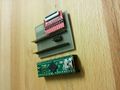
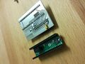
Teensy++ 2.0


Description[edit | edit source]
The Teensy is a complete USB-based microcontroller development system, in a very small footprint, capable of implementing many types of projects. All programming is done via the USB port. No special programmer is needed
To use it as a PS3 flasher is needed to program it with either NORway.hex or NANDway.hex, explained below
- Teensy++ 2.0 dimensions: (1 decimal rounded)
- PCB length - 5 centimeter (2.0 inch)
- PCB width - 1.7 centimeter (0.7 inch)
- PCB thick - 1.5 milimeter
- PCB + Atmel thick - 2.4 milimeter
- PCB + button thick - 3.6 milimeter
- PCB + USB connector thick - 5.7 milimeter
- PCB + USB connector + regulator thick - 7.2 milimeter
Teensy Related Software[edit | edit source]
Teensy drivers[edit | edit source]
Teensy 2.0++ needs windows drivers and linux udev rules to be recognized fully as it was meant to, as explained here http://www.pjrc.com/teensy/usb_serial.html
- Windows driver: serial_install.exe
- Linux UDEV rules: 49-teensy.rules
- FreeBSD device conf: freebsd-teensy.conf
Teensy loader[edit | edit source]
Program used to load the compiled hex-file for the Teensy++ 2.0 microcontroller (AT90USB1286), as explained here: http://www.pjrc.com/teensy/loader.html
- Windows: teensy.exe
- Ubuntu linux x32: teensy.gz
- Ubuntu linux x64: teensy.64bit.gz
- Mac OS-X: teensy.dmg
- Raspberry Pi (experimental): teensy_raspberrypi.tar.gz
- Command line source code on github: https://github.com/PaulStoffregen/teensy_loader_cli
Loading programs to teensy microcontroller[edit | edit source]
See the project home: NORway git, (previously NORway-and-NANDway but now merged in main git)
And download the whole git project from: master.zip
Choose one of the programs needed to be loaded to the teensy to use it as a PS3 flasher (based on your flash type and/or installation type and wiring):
- NORway.hex (for NOR flash PS3 models)
- NANDway_DualNANDEdition.hex (for NAND flash PS3 models with both NANDS connected to teensy)
- NANDway_SignalBoosterEdition.hex (for NAND flash PS3 models with a single NAND connected to teensy)
PC Clients[edit | edit source]
- To run the PC clients in windows (NORway.py or NANDway.py) is needed to install Python and Pyserial
- Python 2.7.2 : python-2.7.2.msi
- Pyserial 2.5 : pyserial-2.5.win32.exe
NORway.py[edit | edit source]
Usage:
C:\>NORway.py
NORway.py v0.8 - Teensy++ 2.0 NOR flasher for PS3 (judges@eEcho.com)
(Original noralizer.py by Hector Martin "marcan" <hector@marcansoft.com>)

Usage:
C:\NORway.py serialport [command] [filename] [address]

  serialport             Name of serial port to open (eg. COM1, COM2, /dev/ttyACM0, etc)
  command  dump          Reads entire NOR to [filename]
           erase         Erases one sector/block (128KB/64KB/8KB) at [address]
           erasechip     Erases entire NOR
           write         Flashes (read-erase-modify-write) [filename] at [address] to NOR (buffered programming mode)
           writeword     Flashes (read-erase-modify-write) [filename] at [address] to NOR (word programming mode)
           writewordubm  Flashes (read-erase-modify-write) [filename] at [address] to NOR (word programming/unlock bypass mode)
           vwrite        Flashes (read-erase-modify-write-verify) [filename] at [address] to NOR (buffered programming mode)
           vwriteword    Flashes (read-erase-modify-write-verify) [filename] at [address] to NOR (word programming mode)
           vwritewordubm Flashes (read-erase-modify-write-verify) [filename] at [address] to NOR (word programming/unlock bypass mode)
           verify        Verifies NOR content with [filename] at [address]
           release       Releases NOR interface, so the PS3 can boot
           bootloader    Enters Teensy's bootloader mode
  filename               Filename for [dump|(v)write|(v)writeword|(v)writewordubm|verify]
  address                Address for [erase|(v)write|(v)writeword|(v)writewordubm|verify]. Default is 0x0, address must be aligned (multiple of 0x20000)

Examples:
  C:\NORway.py COM1
  C:\NORway.py COM1 dump d:\myflash.bin
  C:\NORway.py COM1 erase 0x20000
  C:\NORway.py COM1 erasechip
  C:\NORway.py COM1 write d:\myflash.bin
  C:\NORway.py COM1 write d:\myflash.bin 0xA0000
  C:\NORway.py COM1 writeword d:\myflash.bin
  C:\NORway.py COM1 writewordubm d:\myflash.bin 0x40000
  C:\NORway.py COM1 verify d:\myflash.bin
  C:\NORway.py COM1 release
- For Mac OS-X users with problems of timeouts there is an unnofficial patch available in Discussion page
NANDway.py[edit | edit source]
Usage:
C:\>NANDway.py
NANDway v0.64 - Teensy++ 2.0 NAND Flasher for PS3/Xbox/Wii
(Original NORway.py by judges <judges@eEcho.com>)
(Original noralizer.py by Hector Martin "marcan" <hector@marcansoft.com>)

Usage:
NANDway.py Serial-Port 0/1 Command

  Serial-Port  Name of serial port to open (eg. COM1, COM2, /dev/ttyACM0, etc)
  0/1  NAND id number: 0-NAND0, 1-NAND1
  Commands:
  *  info
     Displays information about NAND
  *  dump Filename [Offset] [Length]
     Dumps to Filename at [Offset] and [Length]
  *  vwrite/write Filename [Offset] [Length]
     Flashes (v=verify) Filename at [Offset] and [Length]
  *  vdiffwrite/diffwrite Filename Diff-file
     Flashes (v=verify) Filename using a Diff-file
  *  ps3badblocks Filename
     Identifies bad blocks in Filename (raw dump)
  *  bootloader
     Enters Teensy's bootloader mode (for Teensy reprogramming)

     Notes: 1) All offsets and lengths are in hex (number of blocks)
            2) The Diff-file is a file which lists all the changed offsets of a dump file. This will increase flashing time dramatically.

Examples:
  NANDway.py COM1 0 info
  NANDway.py COM1 0 dump d:\myflash.bin
  NANDway.py COM1 1 dump d:\myflash.bin 3d a0
  NANDway.py COM1 0 write d:\myflash.bin
  NANDway.py COM3 1 write d:\myflash.bin 20 1c
  NANDway.py COM3 0 vwrite d:\myflash.bin
  NANDway.py COM3 1 vwrite d:\myflash.bin 8d 20
  NANDway.py COM4 0 diffwrite d:\myflash.bin d:\myflash_diff.txt
  NANDway.py COM3 1 vdiffwrite d:\myflash.bin d:\myflash_diff.txt
  NANDway.py COM1 0 bootloader
  NANDway.py ps3badblocks d:\myflash.bin
Notes:
- WP: When the NANDs are mounted on the PS3 motherboard - the WP controllines are already connected to +3.3V. If Teensy is used for NANDs on the PS3 motherboard - the WP wire for each NAND can be discarded.
- Vcc: Teensy 3.3V regulator cannot power the NANDs on the PS3. The drain of the motherboard summed by the other peripherals draw too much current (~1.8A). The NANDs can be powered from external 3.3V power supply like ATX power supply (the orange 3.3V line of the ATX main connector).
Others[edit | edit source]
WAY-launchers[edit | edit source]
Simple GUI to run NORway, NANDway and SPIway.
Project home:
Forum threads:
- http://www.psx-place.com/ps3-news/1793/waylaunchers-now-with-linux-amp-mac-support-by-littlebalup.html
- http://www.psx-place.com/ps3-news/329/waylaunchers-v202-a-gui-to-run-norway-nandway-amp-spiway-scripts.html
- http://www.psx-place.com/forum/downgrading/launchers-325.html
norpatch.exe[edit | edit source]
Small tool to verify content of NOR dump (recognizes any OFW), replace ros0/ros1 with new core os (.NET 2.0 required)
Dump integrity validators[edit | edit source]
See also: Validating flash dumps
Pre-Installation Requirements[edit | edit source]
= Tools[edit | edit source]
The following is a list of suggested good tools and parts you could use to perform the installation of the Teensy++ 2.0 in a PS3
- PS3 disassembling tools:
- 1x Regular Philips head screwdriver
- 1x Torx T-10 or T-8 screwdriver (depending on PS3 model)
- Case modification tools:
- 1x Cutting knife (to make straight cuts in the plastic)
- 1x Drill and small drill bits set
- 1x Needle file set (also known as diamond files for jewellry or hobbyists) with shapes as rounded, squared, triangular, etc. (to make holes in the plastic case or metals with different shapes)
- 1x Dremel tool or similar (to make long straight cuts, not needed on some models)
- 1x Roll of double sided foam tape, or double side thermal resistant tape over 300°C (known as polyimide or kapton tape)
- Soldering work tools:
- 1x Soldering iron (15-30 Watt, or around 230°C) with a 1 millimetre tip
- 1x Tin solder (60/40 or a low melting point 63/37 alloy) with a high percentage of flux core like 2%)
- 1x 30AWG or 26 AWG silver-plated solid core and thermal resistant insulated wrapping wire, also known as kynar wire. (Few have reported 30AWG may be too small and has interference but does work if done well.)
- 1x Cutting knife (to peel wire tips by cutting around them), or a wire stripper tool
- 1x Multimeter (to identify shorts, to identify bad cold solder joints, to find where copper traces in the motherboard are connected, etc.)
- 1x Desoldering braid (aka desoldering wick or solder wick) preferred more than 2 millimetre wide (to fix the mistakes by melting the tin and wicking it, to remove the factory lead-free solder, to clean solders joints where a bad tin alloy happened because residues or degradation of the tin, to remove bridges between pins or pads, etc.)
- 1x Single side thermal resistant tape over 300°C, known as polyimide or kapton tape (to stick wires in place, and other uses)
- 1x Single side aluminium tape (glued), or alufoil (not glued), to create interference shields 1 2 for data wires and to cover PCB's (aluminium protects against interferences but is conductive for this reason is needed to isolate aluminium layers at top and bottom with non-conductive layers as kapton to avoid shorcuts, like a sandwich). Note for correct shielding of wires the shield needs to be connected to ground in both extremes of the "cable" and is posible to solder in aluminium tape
- 1x Fiberglass Scratch Brush or alternatively sandpaper and a needle (to expose vias by removing the green varnish masking layer that covers both sides of the motherboard, needed for some alternative points in NAND motherboards installations)
- 1x Bottle of flux, lead-free, no-clean
- 1x Bottle of 99% Isopropyl alcohol, aka Isopropanol (to clean residues from rosin core of tin, or flux)
- 1x Box of cotton swabs / Q-tips (to spread flux, or clean with alcohol where needed.)
- Other helpers:
- 1x Good lighting (either very well lighted room or a lamp. You need to be able to check your work.)
- 1x Magnifying glass, or jewellry magnifier, preferred 50x zoom (to check your soldering joints for bad cold solders.)
- 1x Small tweezers with a wide tip (to grab wires very close to the tip while soldering them and not burning your fingers in the process, only needed when the solder joint requires extreme precision)
- 1x Pair of steady hands (not joking. tremor fingers will not cut it. You are soldering 40+ points and all must be done very well.)
- 20x of patience, if you are having lot of problems is a good idea to stop and continue another day
As you can see it requires a lot of materials to perform this kind of job. If you do not already have the parts for this kind of project, it will probably be cheaper to pay someone else to do it and ship it to and from them. Also if you are not confident in your soldering technique, it is a very realistic possibility that you will damage your PlayStation 3 Console during this process as there are a LOT of soldering joints that need to be perfectly made.
Install options[edit | edit source]
Powering options[edit | edit source]
Atmel AT90USB128 typical bus powered application with 3V I/O
Atmel AT90USB128 typical bus powered application with 5V I/O


The Atmel AT90USB1286 microcontroller on the teensy has a voltage operation range from 2.7v up to 5.5v, but the same voltages that feeds the teensy are used in the data lines (traveling along the wires connected to PS3 flash)
All PS3 flash models included NAND and NOR works at a range of around 3 volts
For this reason is mandatory to cut the 5v trace at the bottom of the teensy board to feed the teensy with 3.3v, this way teensy and the PS3 flash chips will work at the same 3.3 voltage levels


Teensy powered by USB with onboard voltage regulator[edit | edit source]
Cut the 5V bridge and solder the voltage regulator on the Teensy, then join the 3V bridge as shown in the picture.
With this method there is no need to provide the teensy with external power on the 5v pin next to B6 pin. It will get its power from the usb cable and convert it to 3.3v with the regulator to power the teensy logic.

Teensy powered externally by PS3 or PSU/adaptor[edit | edit source]
After cutting the 5v bridge, solder the 3V bridge, in order to feed the teensy with the 3.3v are several options. Using either an external power supply taking a 3.3v line from the power supply or from a 3.3v point of the PS3 motherboard and connecting it to the +5V pad in a corner of the teensy. Note using a on/off switch in this wire is suggested otherway teensy will be powered up permanently.

Tristate options[edit | edit source]
Tristate, or as it is referred to in the service manuals SB_DISABLE exists solely for the purpose of placing the South Bridge pins into high-impedance (aka the third state logic) so that we can access the flash without the South Bridge interfering.
When the southbridge pins are in tristate is like if southbridge (and all peripherals connected to it) where disconnected from the main circuit, the PS3 powers up normally (fans, etc) but it won't boot up to the XMB screen because some components of the motherboard are not found, it just sits there with a black screen
Because the tristate pin is not connected to the Flash TSOP package, but to the South Bridge BGA package, this makes tracing the pin quite difficult. One should be able to locate it by having the running you could ground out the unknown pins whilst checking the continuity of a known address or data line against ground. These should enter high-impedance or no-continuity when you ground out SB_DISABLE.
= Tristate Question[edit | edit source]
Q: Just one thing, those anyone know if the teensy sets automatically Tristate to ground on version v0.64 without any usb plugged in?
A: No, NORway grounds tristate when you plug it into usb.
But depending on how you power Teensy you might observe some unwanted behaviour that can lead to interference with the console when Teensy is wired up:
- 1. Teensy is powered externally (by console, no vreg)
- When usb is connected, console won't boot, because tristate gets grounded (by design)
- When usb is disconnected, console will boot. Everything's peachy
- 2. Teensy is powered by usb (vreg installed)
- When usb is connected, console won't boot, because tristate gets grounded (by design)
- When usb is disconnected, Teensy isn't powered by usb anymore, but might receive some voltage through signal lines, which can lead to unpredictable behaviour because Teensy is running in an undefined state
LED options[edit | edit source]
http://www.psx-place.com/forum/downgrading/launchers-325-post25084.html#post25084
Removing onboard teensy LED[edit | edit source]
Teensy has an onboard led connected to D6 data line, the led blinks only when there is activity on the D6 line
There is no other software control over the onboard led, if teensy does a write/read on other data lines (not D6) the led is not going to blink
Following the schematics for the led is posible to add one more led for every data line. But this is not a good idea, has been discussed and reported that the onboard led is problematic and can cause reading/writing problems, so adding more leds is just going to cause even more problems, actually the best thing you can do with the onboard leds is to disable it
To disable the led is posible to desolder it, or desolder its resistor, but technically the best way is by cutting its trace because we dont want the led but we dont want the trace either (a trace that goes nowhere is a bad idea and can cause interferences)
The best place to make the cut is at bottom of teensy cutting around the D6 pad, the trace that goes out of D6 pad at bottom is specific for the led. WARNING: dont cut the trace at top of the teensy that connects D6 pad with the atmel chip !
Adding an extra LED for teensy[edit | edit source]
Starting at norway v0.8 has been added a new function to controll an external led connected to pad B7 of teensy
This external LED emits blinks much more informative than the onboard LED, is intended to give much better feedback to the user, it does a flash blink when teensy connects to the PC client (norway.py) at the same time it shows the version on the PC, also the blinking when reading/writing operations are performed is now accurate
This new led functions mapped to pad B7 allows to move the led to any place, handy for permanent installations of teensy because you can place the led on the outside of the PS3 case to see how it blinks, or you can repurpose one/some of the original leds of the PS3 case to be controlled by teensy, as explained here: HSW-001 Contour backlight controlled by teensy
Pinouts and schematics[edit | edit source]
Pinouts by flash type[edit | edit source]
See Hardware flashing page
| Flash Type / Model | PS3 Fat | PS3 Slim | PS3 SuperSlim | notes | |||||||||||||||||
|---|---|---|---|---|---|---|---|---|---|---|---|---|---|---|---|---|---|---|---|---|---|
| CECHA CECHB |
CECHC CECHE |
CECHE | CECHG | CECHH CECHM CECHQ |
CECHJ CECHK |
CECHL CECHP |
CECH-20xx | CECH-21xx | CECH-25xx | CECH-25xx | CECH-30xx | CECH-40xxB/C | CECH-40xxB/C | CECH-40xxA '12GB' noHDD | |||||||
| COK 001 |
COK 002 |
COK 002W |
SEM 001 |
DIA 001 |
DIA 002 |
VER 001 |
DYN 001 |
SUR 001 |
JTP 001 |
JSD 001 |
KTE 001 |
MSX 001 |
MPX 001 |
MPX 001 | |||||||
| NAND | 2x Samsung K9F1G08U0A-PIB0 | Yes | Yes | Yes | - | No | No | No | No | No | No | No | No | No | No | No | |||||
| 2x Samsung K9F1G08U0B-PIB0 | - | - | - | Yes | No | No | No | No | No | No | No | No | No | No | No | ||||||
| NOR | 1x Spansion S29GL128N90TFIR2 | No | No | No | No | Yes | Yes | Yes | Yes | - | - | - | - | - | - | No | |||||
| 1x Samsung K8Q2815UQB-PI4B | No | No | No | No | - | - | Yes | Yes | Yes | - | - | - | - | - | No | ||||||
| 1x Spansion S29GL128P90TFIR2 | No | No | No | No | - | - | Yes | Yes | Yes | Yes | Yes | Yes | Yes | Yes | No | ||||||
| 1x Macronix MX29GL128ELT2I-90G | No | No | No | No | - | - | - | Yes | Yes | Yes | yes ? | Yes | No | ||||||||
| 1x Samsung K8P2716UZC-QI4D | No | No | No | No | Yes | - | - | - | - | Yes | Yes | Yes | No | ||||||||
| 1x Macronix MX29GL128FLT2I-90G | No | No | No | No | - | - | - | - | - | - | - | - | Yes | Yes | No | ||||||
| eMMC | 1x Panasonic MN66840 + 1x Samsung KLMAG2GE4A-A001 |
No | No | No | No | No | No | No | No | No | No | No | No | No | No | Yes | |||||
| connection type | NAND layout 1 | NOR layout 1 | NOR layout 2 | NOR layout 3 | NOR layout 4 | NOR layout 5 | eMMC layout | ||||||||||||||
NORway[edit | edit source]

NANDway Dual NAND Edition[edit | edit source]

NANDway Signal Booster Edition[edit | edit source]

Schematics by motherboard (retail)[edit | edit source]
The official purpose of this testpoints is to connect the motherboard to a JIG machine that uses adapters with Pogo pins
NAND layout 1[edit | edit source]
Labeled with motherboard testpoint names
COK-001 boardtraces (NAND board) confirmed
COK-002 boardtraces (NAND board) confirmed
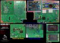
SEM-001 boardtraces (NAND board) confirmed


NOR layout 1[edit | edit source]
Labeled with motherboard testpoint names
DIA-001 NOR Testpoints (NOR layout 1)
DIA-002 NOR Testpoints (NOR layout 1)


NOR layout 2[edit | edit source]
Labeled with teensy pad names
Schematic for VER-001 - Teensy 2++ with External Power Only

Labeled with motherboard testpoint names
VER-001 NOR Testpoints (NOR layout 2)
VER-001 NOR Testpoints - trisaster.de, missing Tristate (NOR layout 2)


NOR layout 3[edit | edit source]
Labeled with motherboard testpoint names
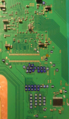
DYN-001 NOR Testpoints (NOR layout 3)
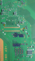
DYN-001 NOR Testpoints + dualboot 'AB mod' (NOR layout 3)
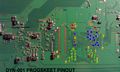
DYN-001 NOR Testpoints with progskeet labeling (NOR layout 3)


NOR layout 4[edit | edit source]
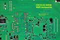
Labeled with teensy pad names
Teensy++2.0 NOR testpoints layout 4
Teensy++2.0 SUR-001 NOR testpoints
Teensy++2.0 JTP-001 NOR testpoints
Teensy++2.0 JSD-001 NOR testpoints
Teensy++2.0 KTE-001 NOR testpoints
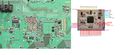
JSD-001, Teensy++ 2.0 Connection Diagram


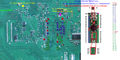
Labeled with motherboard testpoint names
JSD-001, JTP-001, KTE-001 NOR Testpoints with Progskeet labeling (NOR layout 4)
JSD-001, JTP-001, KTE-001 NOR Testpoints with Progskeet 1.2 labeling (NOR layout 4)
JSD-001 NOR Testpoints (NOR layout 4)
JSD-001 Testpoints - orig. marcan/noraliser (NOR layout 4)


Schematics by motherboard (non retail)[edit | edit source]
NOR DEB-001[edit | edit source]
Teensy++ 2.0 DEB-001 NOR testpoints

Teensy Solder Install Notes by Motherboard Model[edit | edit source]
First open the PS3. Follow youtube videos to learn how (Just search).
Once opened, look at the motherboard model printed there. Depending on which model you have follow the case modifications below to install teensy.
There are two methods to use a Teensy 2.0++ Flasher.
1.) Install while the PS3 is somewhat opened still with everything plugged in. (Be careful of shorts.)
2.) Internal Case Modifications. This is the best way to go as you can install the teensy inside of the PS3 for later use. This is the advantage of using a Teensy 2.0++ because it's just small enough to install inside the PS3 with a little case modification. Other flashers are generally too large to do this with the PS3 closed up. You will find there is just no room for it.
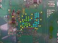
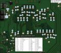
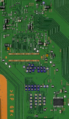
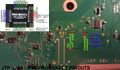
COK-001, COK-002, COK-002W, SEM-001[edit | edit source]
I used the image for the Progskeet, along with an image of which Progskeet pin(GP1 etc.) corresponds to which NAND chip pin name (WP, ALE, CLE, I/O1 etc.) to create a diagram of which testpoint on the mainboard goes to which leg of the NAND chips made by Samsung.

So now you can use this diagram not only for downgrading/dumping/writing the NANDs with a Teensy++ 2.0 board, but with any other board available on the Internet.
Important: You must provide a stable 3.3V PSU to both the PS3 board and the Teensy, and don’t forget to unite the GNDs. You can use any PSU which outputs 3.3V @ 1.8A+, the easiest option will be to use a PC PSU.
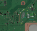
DIA-001, DIA-002[edit | edit source]
Parts not needed? Submitter please list here.
Installation and Case Modification[edit | edit source]
This installation the case was not modified. It was flashed while opened, and removed.


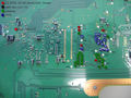
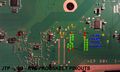
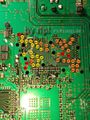
VER-001[edit | edit source]
Usage :
1 - Connect first SB VCC 2v Max
2 - Connect in second step Vcc Teensy2++ 3.3v
Schematic for VER-001 - Teensy 2++ with External Power Only
Installation and case modification[edit | edit source]
In this installation, the cables were strategically soldered to fit better and not break or short when the power supply was placed, so no external power was needed.


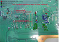
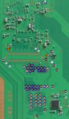
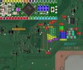
DYN-001[edit | edit source]
Parts not needed - Torque T-10 Screwdriver. (T-8 IS still needed!)
Installation and Case Modifications[edit | edit source]
Be sure to make a screw map when disassembling the PS3, there are a lot of screws, and you will not remember where they go.
First and Second dremel area. These 4 pictures show before and after affects and where to dremel on the top side shielding.


Third dremel area. These pictures show before and after affects and where to dremel on the bottom side shielding.
This helps with interference by running wires outside the shielding instead of inside. This method has to be done
on these models as unlike JSD-001 Models there are no holes or spaces between the HDD and shielding. It's connected
on DYN-001 Models.
NOTE: When placing teensy, DO NOT PLACE directly on the shielding. Make sure you use a strip of double sided foam tape. to act between the shielding and teensy.


Forth and last dremel area. This is done on the case itself. The port for the teensy is covered by the HDD cover area. You will have to take care in cutting open the area. If you did not spread your wires out evenly on the underside of the shielding, it will create a raised section and the port itself will be too high to reach and may have to dremel higher.


Notes on Reassembly: Before putting back the blu-ray drive, carefully bend each wire on the topside flat by hand ONE AT A TIME so you do not break the solder joints on the teensy. If you do not bend them flat by hand one at a time carefully, the drive could easily undo one of your soldering joints and you will have to start again. (I managed to do it on the first try. Did I say that you needed 1x of Patience?
Testing: You can test your work before putting the cover top back on. Just make sure blu-ray and power-supply are connected and everything else before trying. This is so you know that everything is fitting okay and that the install has worked for you. Take 3 dumps (Read above on how to take a dump of NOR) and compare them. Do md5sum and sha1sum, and then try and unpack them with norunpack from f0f tools. If they all match, and it unpackages, congratulations you have a good dump!
JSD-001[edit | edit source]
No dremel required. Design of this CECH 2500 series has an opened hole area to put wires through.
Installation and Case Modification[edit | edit source]


SUR-001/JTP-001/KTE-001[edit | edit source]
- Need submissions...
Teensy Flash Clip adapters[edit | edit source]
Teensy clip adapter Board for NANDway v1[edit | edit source]
Layout for a PCB without external Voltage-source (this was the first version without capacitors, Voltageregulator and two bridges)
deprecated, use v2 instead
Gallery[edit | edit source]
Teensy adapter Board for NANDway v1 - top
Teensy adapter Board for NANDway v1 - bottom


Download[edit | edit source]
Teensy2Clip - Folie.pdf mirror
Teensy clip adapter Board for NANDway v2.1[edit | edit source]
Allows to connect a Teensy++ 2.0 to a 360-NAND Clip
Source article: http://playstationhax.it/forums/topic/1149-teensy-adapter-board-for-nandway/


Hey. in the past, i create a simple adapter board to connect the Teensy to a "360-clip NAND Clip" (the classic kind of NAND Clips). It's easier and faster to solder a board than wire the cables, no more problems with cable breaks and a good connection. An english speaking user ask me for a solder tutorial, so I thought on this occasion, i can write directly to the community. :) Of course, you can find all what you need below to order your own boards.
I hope i could help someone
with kind regards
esprit1711 from psXtools Team :)
But now the tutorial with some words (the most things should be self-explanatory).
What you need[edit | edit source]

- 1x adapter board
- 1x Teensy++ 2.0
- 1x 5V to 3,3V Voltage Regulator for the Teensy (MCP1825, LM3940 or Pin-compatible)
- 1x TSSOP 48 NAND-Clip (360-Clip) with equipment (Flat-cable, Pin-header (2x11) and the red adapter board (you get always all these things when you buy a new NAND Clip)
- 2x Pin-header (1x20)
- 1x Pin-header (2x4)
optional but recommendable[edit | edit source]
- 2x female connector (1x20)
- 1x female connector (2x4)
- 1x Pin-header (1x3)
- 1x Jumper
- 1x Capacitor 100nF SMD-0603
- 1x Capacitor 10µF SMD-0805
Optional (if you want power the NAND with external Power)[edit | edit source]
- 1x 5V to 3,3V Voltage Regulator (LMS1587CS-3.3 or Pin-compatible)
- 1x 5V Powersupply (minimum 3A)
See section above to cut the 5v trace on teensy and how to solder the 3.3v regulator at the bottom of teensy board
Solder the adapter board[edit | edit source]
Solder pinheaders on adapterboard[edit | edit source]
Solder the pin-header on the board (be careful, the plastic of the pin-header could melt fast)

now, plug the red adapter board (which was at the NAND-clip) on the pin-header, solder the pins and cut them if they are too long.
Solder adapterboard on pinheader[edit | edit source]

Mount Teensy to board[edit | edit source]
You can choose, if you want solder the Teensy fixed on the board....

... or solder the Teensy on female connector to unplug him any time

Powersource 1x3 pinheader[edit | edit source]
with the following 1x3 pin-header, you can choose the Powersource for the NAND (external, or USB) (sometimes it can cause problems, when you use the USB as Power Supply)

when you Power the NAND by USB, the final step is to connect the common header-pin with outermost pin

Optional things:[edit | edit source]
Filtering[edit | edit source]
for a cleaner voltage, you should solder the capacitors


External regulator[edit | edit source]
you can also solder a stronger voltage-regulator (than the one on the Teensy) to connect a stronger 5V power supply (than your USB Port).
Before you solder the regulator on the board, you should prepare the large pad of the Regulator and the Board with a layer of tin.


DC connector[edit | edit source]
you can connect your 5V Power supply on the marked solder points. I used a DC-coupling for a better handling

when you want use the external voltage, you must reposition the jumper (like you can see on the picture), but you can always change the powersource with the jumper
Where you can buy this boards?[edit | edit source]
You can find a zip-file to download below. in this file, you find the complete project folder. You can use the files to view and change the Layout or the circuit diagram, but if you only want a board, you can send this zip-file to a PCB service. I order my boards always at elecrow.com. The board has a size of 55mm x 45mm, so you must order the boards on this page.
Before you add your order to the cart, the options should (except the colour, this is your choice) look like on the following picture (a change of the order quantity only changed the weight and the transportation costs, so i order always 10 boards)

= Download[edit | edit source]
Teensy Adapter Platine V2.zip / mirror
 EDIT 2015-06-10
 V2.1 available / 2.1 mirror.
 Fixed a layout mistake (twisted the 2x4 pin header at the Teensy socket (thank to Th3Knights for the report)
 and change the silkscreen. If you have a V2, you can use it without any problem. the V2 use only 2 of 5 lines
 for RE, but this is not a critical problem.
You can open the project file with Target3001 (the simplest variant of this tool is free), but below, you find a pdf of the schematic, too
Teensy Adapter Platine V2.pdf mirror
TEENSY2PS3[edit | edit source]
http://www.psx-place.com/forum/downgrading/teensy2ps3-pcb-linker-teensy-2-0-ps3-1728.html
http://www.mediafire.com/download/i9tma7gkft84442/TEENSY2PS3_v1.00.zip
Offboard flashing[edit | edit source]
Using flash ZIF sockets
TSOP48 ZIF socket (for NAND)[edit | edit source]
TSOP56 ZIF socket (for NOR)[edit | edit source]
- REMARK >> WP(pin 16) to Vcc and BYTE(pin 53) to Vcc
Teensy Official Distributors[edit | edit source]
https://forum.pjrc.com/threads/23601-Official-Distributors
- PJRC (USA, Oregon) : http://www.pjrc.com/store/teensypp.html + http://www.pjrc.com/store/mcp1825.html
- Adafruit (USA, New York) : http://www.adafruit.com/products/731 +
- Floris.cc (Netherlands) : http://floris.cc/shop/en/teensy/951-teensy-20-usb-development-board.html + http://floris.cc/shop/en/teensy/89-mcp1825s-33-volt-voltage-regulator-for-teensy-2.html
- MindKits (New Zealand) : http://www.mindkits.co.nz/store/arduino-compatible/teensy-2-0 + ? http://www.mindkits.co.nz/store/components-ics-breakout-boards/voltage-regulator-3v3 (not SOT-223) or http://www.mindkits.co.nz/store/components-ics-breakout-boards/voltage-regulator-adjustable-lm1117-smd (not fixated: requires two external resistors for trimming it to 3.3V)
- HiTech Store (Germany) : http://www.hitechstore.de/produkt/teensypp/ + http://www.hitechstore.de/produkt/mcp1825s33/
- Watterott (Germany) http://www.watterott.com/de/Teensy-v20-AT90USB1286
- Boxtec (Switzerland) : http://shop.boxtec.ch/teensy-board-p-40725.html + ? http://shop.boxtec.ch/ams1117-voltage-regulator-p-40516.html out of catalog
- Teague (as part of Teagueduino) : no stock
- Sound Art Lab (South Korea) : no stock
- Little Bird Electronics (Australia) : http://littlebirdelectronics.com.au/products/teensy-2-0
- Hobbytronics (UK) : http://www.hobbytronics.co.uk/teensy-pp2
- Proto-pic (UK) : http://proto-pic.co.uk/teensy-2-0/
- PT-robotics (Portugal) : http://www.ptrobotics.com/modulos-teensy/2539-teensy-20.html
| ||||||||||||||||||||||||||||||||||||||