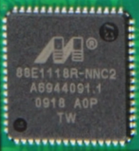
88E1118R-NNC2
Jump to navigation
Jump to search
Marvell Alaska 88E1118R-NNC2 (Ethernet Controller)
productcode meaning:
88E1118R-NNC2 = 10/100/1000BASE-T PHY with RGMII

Type: Ethernet
Speed : 1Gbps
VCC: 1.8V (regulators can be supplied with 1.8V, 2.5V or 3.3V)
I/O: 1.8V, 2.5V or 3.3V
125MHz Clock input
Package : 64-pin QFN

(sorry, no explaination yet)
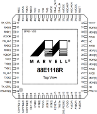
Pinout 64-pin QFN
| Pin # | Name | Pin Type | Description |
|---|---|---|---|
| 1 | CONFIG[1] | I | Hardware Configuration |
| 2 | CONFIG[2] | I | Hardware Configuration |
| 3 | CONFIG[3] | I | Hardware Configuration |
| 4 | CLK125 | O | 125 MHz Clock Output. When Hardware reset is asserted, a 25 MHz clock is generated output, otherwise a 125 MHz clock is output. |
| 5 | DVDD | Power | Digital core supply - 1.2V. DVDD can be supplied externally with 1.2, or via the 1.2V regulator. |
| 6 | LED[0] | O | LED/Interrupt outputs |
| 7 | VDDO | Power | 1.8V, 2.5V, or 3.3V non-RGMII digital I/O supply. VDDO must be supplied externally. Do not use the 1.8V regulator to power VDDO. |
| 8 | LED[1] | O | LED/Interrupt outputs |
| 9 | LED[2] | O | LED/Interrupt outputs |
| 10 | RESETn | I | Hardware reset. Active low. 0 = Reset 1 = Normal |
| 11 | TRSTn | I, PU | Boundary scan test reset input. Active low. TRSTn contains an internal 150 kohm pull-up resistor as per the 1149.1 specification. After power up, the JTAG state machine should be reset by applying a low signal on this pin, or by keeping TMS high and applying 5 TCK pulses, or by pulling this pin low by a 4.7 kohm resistor. |
| 12 | DIS_REG12 | I | 1.2V Regulator Disable. Tie to VDDO to disable, tie to VSS to enable. |
| 13 | DVDD | Power | Digital core supply - 1.2V. DVDD can be supplied externally with 1.2, or via the 1.2V regulator. |
| 14 | AVDDR | 1.2V Regulator supply - 1.8V AVDDR can be supplied externally with 1.8V, or via the 1.8V regulator. If the 1.2V regulator is not used, AVDDR must still be tied to 1.8V. | |
| 15 | AVDDR | 1.2V Regulator supply - 1.8V AVDDR can be supplied externally with 1.8V, or via the 1.8V regulator. If the 1.2V regulator is not used, AVDDR must still be tied to 1.8V. | |
| 16 | AVDDX | Power | 1.8V Regulator supply - 2.5V, 3.3V, (or 1.8V). AVDDX must be supplied externally. Note that this supply must be the same voltage as AVDDC. If the 1.8V regulator is not used, then it means a 1.8V supply is in the system. AVDDX (along with AVDDC) would be tied to 1.8V in this case. |
| 17 | CTRL18 | O | 1.8V Regulator Control. This signal ties to the base of the BJT. If the 1.8V regulator is not used it can be left floating. |
| 18 | NC | NC | No connect. These pins are not connected to the die so they can be connected to anything on the board. |
| 19 | MDIN[3] | I/O, D | Media Dependent Interface[3] |
| 20 | MDIP[3] | I/O, D | Media Dependent Interface[3] |
| 21 | AVDD | Power | Analog supply. 1.8V. AVDD can be supplied externally with 1.8V, or via the 1.8V regulator. |
| 22 | AVDD | Power | Analog supply. 1.8V. AVDD can be supplied externally with 1.8V, or via the 1.8V regulator. |
| 23 | MDIN[2] | I/O, D | Media Dependent Interface[2] |
| 24 | MDIP[2] | I/O, D | Media Dependent Interface[2] |
| 25 | MDIN[1] | I/O, D | Media Dependent Interface[1] |
| 26 | MDIP[1] | I/O, D | Media Dependent Interface[1] |
| 27 | AVDD | Power | Analog supply. 1.8V. AVDD can be supplied externally with 1.8V, or via the 1.8V regulator. |
| 28 | NC | NC | No connect. These pins are not connected to the die so they can be connected to anything on the board. |
| 29 | AVDD | Power | Analog supply. 1.8V. AVDD can be supplied externally with 1.8V, or via the 1.8V regulator. |
| 30 | MDIN[0] | I/O, D | Media Dependent Interface[0] |
| 31 | MDIP[0] | I/O, D | Media Dependent Interface[0] |
| 32 | TSTPT | O | Test Point |
| 33 | RSET | I | Constant voltage reference. External 4.99 kohm 1% resistor connection to VSS required for each pin. |
| 34 | AVDDC | Analog supply - 1.8V or 2.5V, or 3.3V. AVDDC must be supplied externally. Do not use the 1.8V regulator to power AVDDC. | |
| 35 | HSDACN | O | AC Test Point. Connect the AC testpoints with a 50 ohm termination resistor to VSS for IEEE testing and debug purposes. If debug and IEEE testing are not of importance, these pins can be left floating. |
| 36 | HSDACP | O | AC Test Point. Connect the testpoints with a 50 ohm termination resistor to VSS for IEEE testing and debug purposes. If debug and IEEE testing are not of importance, these pins can be left floating. |
| 37 | AVDDC | Analog supply - 1.8V or 2.5V, or 3.3V. AVDDC must be supplied externally. Do not use the 1.8V regulator to power AVDDC. | |
| 38 | XTAL_IN | I | Reference Clock. 25 MHz ± 50 ppm tolerance crystal reference or oscillator input.
NOTE: If AVDDC is tied to 1.8V, then the XTAL_IN pin is not 2.5V/3.3V tolerant. If AVDDC is tied to 2.5V, then the XTAL_IN pin is not 3.3V tolerant. |
| 39 | XTAL_OUT | O | Reference Clock. 25 MHz ± 50 ppm tolerance crystal reference. When the
XTAL_OUT pin is not connected, it should be left floating. |
| 40 | DVDD | Power | Digital core supply - 1.2V. DVDD can be supplied externally with 1.2, or via the 1.2V regulator. |
| 41 | TMS | I, PU | Boundary scan test mode select input. TMS contains an internal 150 kohm pull-up resistor. |
| 42 | TCK | I, PU | Boundary scan test clock input. TCK contains an internal 150 kohm pull-up resistor. |
| 43 | TDI | I | Boundary scan test data input |
| 44 | TDO | O | Boundary scan test data output |
| 45 | MDIO | I/O | MDIO is the management data. MDIO transfers management data in and out of the device synchronously to MDC. This pin requires a pull-up resistor in a range from 1.5 kohm to 10 kohm. |
| 46 | VDDO | Power | 1.8V, 2.5V, or 3.3V non-RGMII digital I/O supply. VDDO must be supplied externally. Do not use the 1.8V regulator to power VDDO. |
| 47 | DVDD | Power | Digital core supply - 1.2V. DVDD can be supplied externally with 1.2, or via the 1.2V regulator. |
| 48 | MDC | I | MDC is the management data clock reference for the serial management interface. A continuous clock stream is not expected. The maximum frequency supported is 8.3 MHz. |
| 49 | RX_CTRL | O | RGMII Receive Control. RX_DV is presented on the rising edge of RX_CLK. A logical derivative of RX_DV and RX_ER is presented on the falling edge of RX_CLK. |
| 50 | RXD[0] | O | RGMII Receive Data |
| 51 | RXD[1] | O | RGMII Receive Data |
| 52 | VDDOR | Power | 1.8V, 2.5V, or 3.3V RGMII digital I/O supply. VDDOR must be supplied externally. Do not use the 1.8V regulator to power VDDOR. |
| 53 | RX_CLK | O | RGMII Receive Clock provides a 125 MHz, 25 MHz, or 2.5 MHz reference clock with ± 50 ppm tolerance derived from the received data stream depending on speed. |
| 54 | RXD[2] | O | RGMII Receive Data |
| 55 | RXD[3] | O | RGMII Receive Data |
| 56 | VDDOR | Power | 1.8V, 2.5V, or 3.3V RGMII digital I/O supply. VDDOR must be supplied externally. Do not use the 1.8V regulator to power VDDOR. |
| 57 | VREF | I | RGMII input voltage reference. Must be set to VDDOR/2 when used as 1.8V HSTL, 2.5V SSTL_2, and 3.3V. Set to VDDOR when used as 2.5V LV CMOS. |
| 58 | TXD[0] | I | RGMII Transmit Data |
| 59 | TXD[1] | I | RGMII Transmit Data |
| 60 | TCX_CLK | I | RGMII Transmit Clock provides a 125 MHz, 25 MHz, or 2.5 MHz reference clock with ± 50 ppm tolerance depending on speed. |
| 61 | TXD[2] | I | RGMII Transmit Data |
| 62 | TXD[3] | I | RGMII Transmit Data |
| 63 | TX_CTRL | I | RGMII Transmit Control. TX_EN is presented on the rising edge of TX_CLK. A logical derivative of TX_EN and TX_ER is presented on the falling edge of TX_CLK. |
| 64 | CONFIG[0] | I | Hardware Configuration |
| EPAD | VSS | GND | Ground to device. The 64-pin QFN package has an exposed die pad (E-PAD) at its base. This E-PAD must be soldered to VSS. |
| This article is marked for rewrite/restructuring in proper wiki format. You can help PS3 Developer wiki by editing it. |
| |||||||||||||||||||||||||||||||||||||||||||||||||||||||||||||||||||||||||||||||||||||||||||||||||||||||||||||||||||||||||||||||||||||||||||||||||||||||||||||||||||||||||||||


