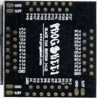
Hardware Flashers:NAND pinout
NAND Consoles[edit | edit source]
These are the earliest revisions of the PS3 motherboards: CECHA/COK-001, CECHB/COK-001, CECHC/COK-002, CECHE/COK-002W, CECHG/SEM-001 and contain 2x NAND chips for a total of 256MB. These chips are interleaved which is controlled by a proprietary controller chip codenamed "Starship2" or SS2. This chip handles the interleaving and presents the NAND Chips to the South Bridge as a single large coherent flash over a proprietary EBUS.
NAND Wiring[edit | edit source]
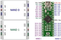
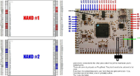
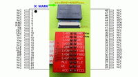
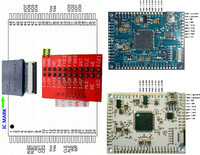
Flashers for NAND based consoles (CECHA/COK-001, CECHB/COK-001, CECHC/COK-002, CECHD/unreleased, CECHE/COK-002W, CECHF/unreleased, CECHG/SEM-001) are generaly wired directly to the pins of the NAND (you cannot use the testpoints! between Southbridge and Starship2), plus ground and Vcc. Alternatively, boardtraces (between Starship2 and NAND) can be used.
Which NAND is low/high?[edit | edit source]
- COK-001 :
- COK-002 + COK-002W :
- IC3802 LOW (main componentside with SATA connector, CELL BE, RSX etc. between SATA connector and South Bridge)
- IC3803 HIGH (main componentside with SATA connector, CELL BE, RSX etc. between SATA connector and AV Multi connector)
- SEM-001 :
EBUS Interface Testpoints on NAND consoles[edit | edit source]
Simular as on the NOR based consoles, testpoints can be found on the back of the PCB. It seems these are from the EBUS between the South Bridge and the Starship2. Attempts have been made to document/trace these. Addresslines 0-17 and Datalines 0-15 as well as some controllines are documented but so far these could not be used to read/flash the console.
TriState on NAND consoles[edit | edit source]
using Starship2 to southbridge /SB_EBUS_ACK @ SB_MAIN(P30) (numbered 52 in File:SS2_NOR.JPG)
- CECHA (COK-001): IC3801:CXD4302GB-T6 pin:C1/ ebus jl:9308 (page 20 of servicemanual)
- CECHC + CECHE (COK-002): IC3801:CXD4302GB-T6 pin:C1/ ebus jl:9308 (page 20 of servicemanual)
- CECHG (SEM001): IC3801:CXD9909GB pin:C1/ ebus jl:9308 (page 21 of servicemanual)
NAND Pinout table[edit | edit source]
| Chip/PIN | Description | NANDway | Progskeet 1.0 / 1.1 S-NAND | Progskeet 1.0 / 1.1 SL-NAND | Progskeet 1.2 / 1.21 | Infectus | 360clip | Description |
|---|---|---|---|---|---|---|---|---|
| NAND 0 | ||||||||
| 0/1-6 | NC | NC | NC | NC | NC | NC | NC | No Connection |
| 0/7 | R/B | PB6 | 64 / rdy | gp5 | P02 | U | FRB1 | Read/Busy Output |
| 0/8 | RE | PB1 | 69 / oe | gp1 | P06 | M | RE | Read Enable |
| 0/9 | CE | PB0 | 60 / gp3 | gp2 | P05(p) CE_A / P03(s) CE_B | N | FCE1 | Chip Enable |
| 1/10+11 | NC | NC | NC | NC | NC | NC | NC | No Connection |
| 0/12 | Vcc | +3.3 | +3.3 | +3.3 | NC | Vcc | Vcc (min 2.7V-max 3.6V / typ 3.3V) | |
| 0/13 | Vss | GND | GND | GND | NC | GND | VSS - Ground | |
| 1/14+15 | NC | NC | NC | NC | NC | NC | NC | No Connection |
| 0/16 | CLE | PB2 | 63 / gp0 | we | P09 | O | CLE | Command Latch Enable |
| 0/17 | ALE | PB3 | 62 / gp1 | rdy | P08 | P | ALE | Address Latch Enable |
| 0/18 | WE | PB5 | 65 / we | gp0 | P07 | Q | WE | Write Enable |
| 0/19 | WP | PB4 | 61 / gp2 | gp3 | P04 | T | WP | Write Protect |
| 1/20-28 | NC | NC | NC | NC | NC | NC | NC | No Connection |
| 0/29 | I/O-0 | PF0 | 79 / dq0 | 79 / dq0 | P34 | D0 | I/O0 | |
| 0/30 | I/O-1 | PF1 | 80 / dq1 | 80 / dq1 | P35 | D1 | I/O1 | |
| 0/31 | I/O-2 | PF2 | 81 / dq2 | 81 / dq2 | P36 | D2 | I/O2 | |
| 0/32 | I/O-3 | PF3 | 82 / dq3 | 82 / dq3 | P37 | D3 | I/O3 | |
| 0/33-35 | NC | NC | NC | NC | NC | NC | NC | No Connection |
| 0/36 | Vss | GND | GND | GND | NC | GND | VSS - Ground | |
| 0/37 | Vcc | +3.3 | +3.3 | +3.3 | NC | Vcc | Vcc (min 2.7V-max 3.6V / typ 3.3V) | |
| 0/38-40 | NC | NC | NC | NC | NC | NC | NC | No Connection |
| 0/41 | I/O-4 | PF4 | 83 / dq4 | 83 / dq4 | P38 | D4 | I/O4 | |
| 0/42 | I/O-5 | PF5 | 84 / dq5 | 84 / dq5 | P39 | D5 | I/O5 | |
| 0/43 | I/O-6 | PF6 | 85 / dq6 | 85 / dq6 | P40 | D6 | I/O6 | |
| 0/44 | I/O-7 | PF7 | 86 / dq7 | 86 / dq7 | P41 | D7 | I/O7 | |
| 0/45-48 | NC | NC | NC | NC | NC | NC | NC | No Connection |
| 0/- | NC | NC | NC | NC | NC | NC | PRE | Not used |
| 0/10 | NC | NC | NC | NC | NC | NC | FCE2 | Not used |
| 0/6 | NC | NC | NC | NC | NC | NC | FRB2 | Not used |
| 0/- | NC | NC | NC | NC | NC | NC | RST | Not used |
| NAND 1 | ||||||||
| 1/1-6 | NC | NC | NC | NC | NC | NC | NC | No Connection |
| 1/7 | R/B | PD6 | 3 / gp13 | a15 | P26 | A9 | FRB1 | Read/Busy Output |
| 1/8 | RE | PD1 | 98 / gp15 | a19 | P30 | A15 | RE | Read Enable |
| 1/9 | CE | PD0 | 7 / gp9 | a18 | P29(p) CE_A / P27(s) CE_B | A14 | FCE1 | Chip Enable |
| 1/10+11 | NC | NC | NC | NC | NC | NC | NC | No Connection |
| 1/12 | Vcc | +3.3 | +3.3 | +3.3 | NC | Vcc | Vcc (min 2.7V-max 3.6V / typ 3.3V) | |
| 1/13 | Vss | GND | GND | GND | NC | GND | VSS - Ground | |
| 1/14+15 | NC | NC | NC | NC | NC | NC | NC | No Connection |
| 1/16 | CLE | PD2 | 4 / gp12 | a22 | P33 | A13 | CLE | Command Latch Enable |
| 1/17 | ALE | PD3 | 5 / gp11 | a21 | P32 | A12 | ALE | Address Latch Enable |
| 1/18 | WE | PD5 | 2 / gp14 | a20 | P31 | A11 | WE | Write Enable |
| 1/19 | WP | PD4 | 6 / gp10 | a17 | P28 | A10 | WP | Write Protect |
| 1/20-28 | NC | NC | NC | NC | NC | NC | NC | No Connection |
| 1/- | NC | NC | NC | NC | NC | NC | PRE | Not used |
| 1/10 | NC | NC | NC | NC | NC | NC | FCE2 | Not used |
| 1/6 | NC | NC | NC | NC | NC | NC | FRB2 | Not used |
| 1/- | NC | NC | NC | NC | NC | NC | RST | Not used |
| 1/29 | I/O-0 | PC0 | 90 / dq8 | 90 / dq8 | P42 | A0 | I/O0 | |
| 1/30 | I/O-1 | PC1 | 91 / dq9 | 91 / dq9 | P43 | A1 | I/O1 | |
| 1/31 | I/O-2 | PC2 | 92 / dq10 | 92 / dq10 | P44 | A2 | I/O2 | |
| 1/32 | I/O-3 | PC3 | 93 / dq11 | 93 / dq11 | P45 | A3 | I/O3 | |
| 1/33-35 | NC | NC | NC | NC | NC | NC | NC | No Connection |
| 1/36 | Vss | GND | GND | GND | NC | GND | VSS - Ground | |
| 1/37 | Vcc | +3.3 | +3.3 | +3.3 | NC | Vcc | Vcc (min 2.7V-max 3.6V / typ 3.3V) | |
| 1/38-40 | NC | NC | NC | NC | NC | NC | NC | No Connection |
| 1/41 | I/O-4 | PC4 | 94 / dq12 | 94 / dq12 | P46 | A4 | I/O4 | |
| 1/42 | I/O-5 | PC5 | 95 / dq13 | 95 / dq13 | P47 | A5 | I/O5 | |
| 1/43 | I/O-6 | PC6 | 96 / dq14 | 96 / dq14 | P48 | A6 | I/O6 | |
| 1/44 | I/O-7 | PC7 | 97 / dq15 | 97 / dq15 | P49 | A7 | I/O7 | |
| 1/45-48 | NC | NC | NC | NC | NC | NC | NC | No Connection |
| Board trace / Other | ||||||||
| GND | Vss | NC | NC | NC | NC | GND | NC | VSS - Ground |
| +5VDC | Vcc | NC | NC | NC | NC | 5V | NC | Vcc from TH3401 (CECHA+CECHB/COK-001) Vcc from TH3401 (CECHC+CECHE/COK-002) Vcc from TH3280 (CECHG/SEM-001) |
| TRISTATE | tri | PB7 / PD7 | NC | NC | NC | NC | NC | Tristate pad on EBUS Testpoints |
| Chip/PIN | Description | NANDway | Progskeet 1.0 / 1.1 S-NAND | Progskeet 1.0 / 1.1 SL-NAND | Progskeet 1.2 | Infectus | 360clip | Description |
Structure[edit | edit source]
There are 2 NAND used, interleaved at 512byte/sector level, giving it a 1024 byte "interleaved sector". Pages are 2kb on each NAND.
| ||||||||||||||||||||||||||||||||||||||
