MX25L25635FMI-10G: Difference between revisions
Jump to navigation
Jump to search
No edit summary |
(better photo) |
||
| Line 7: | Line 7: | ||
=== Pinout === | === Pinout === | ||
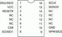
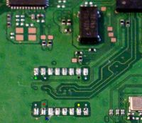
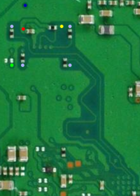
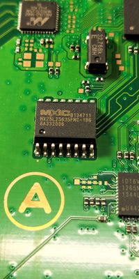
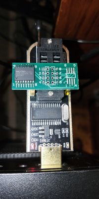
<div style="float:right">[[File:MX25L25635FMI-10G Pinout.png|200px|thumb|left|MX25L25635FMI-10G Pinout]]<br />[[File:8PinWSONCUH1200.png|200px|thumb|left|MX25L25635F-series 8-pin WSON Pinout as found in CUH-12xx-series PS4s]]<br />[[File:MX25L25635FMI-10G Removed - SAA-001 - componentside.jpg|200px|thumb|left|MX25L25635FMI-10G Removed - SAA-001 - componentside]]<br />[[File:MX25L25635FMI-10G - SAA-001 - backside.png|200px|thumb|left|MX25L25635FMI-10G - SAA-001 - backside]]</div> | <div style="float:right">[[File:MX25L25635FMI-10G Pinout.png|200px|thumb|left|MX25L25635FMI-10G Pinout]]<br />[[File:8PinWSONCUH1200.png|200px|thumb|left|MX25L25635F-series 8-pin WSON Pinout as found in CUH-12xx-series PS4s]]<br />[[File:MX25L25635FMI-10G Removed - SAA-001 - componentside.jpg|200px|thumb|left|MX25L25635FMI-10G Removed - SAA-001 - componentside]]<br />[[File:MX25L25635FMI-10G - SAA-001 - backside.png|200px|thumb|left|MX25L25635FMI-10G - SAA-001 - backside]][[File:ps4flash.jpg|200px|thumb|left|MX25L25635FMI-10G Untouched]]</div> | ||
{| border="1" cellspacing="0" cellpadding="5" border="#999" class="wikitable" style="border:1px solid #999; border-collapse: collapse;" | {| border="1" cellspacing="0" cellpadding="5" border="#999" class="wikitable" style="border:1px solid #999; border-collapse: collapse;" | ||
|- bgcolor="#cccccc" | |- bgcolor="#cccccc" | ||
Revision as of 05:15, 11 July 2018
Macronix MX25L25635FMI-10G
3V 256M-BIT [x 1/x 2/x 4] CMOS MXSMIO (SERIAL MULTI I/O) 16-SOP (300mil)
http://datasheet.octopart.com/MX25L25635FMI-10G-Macronix-datasheet-17291205.pdf
Pinout
| Pin | 1x I/O | 2x I/O | 4x I/O | Description | |
|---|---|---|---|---|---|
| S3 | 1 | DNU | DNU | SIO3 | Do not use or Serial Data Input & Output (for 4xI/O read mode) |
| 3.3 | 2 | VCC | VCC | VCC | +3V DC Power Supply |
| RS | 3 | RESET# | RESET# | RESET# | Hardware Reset Pin Active low |
| 4 | NC | NC | NC | No Connection | |
| 5 | NC | NC | NC | No Connection | |
| 6 | NC | NC | NC | No Connection | |
| CS | 7 | CS# | CS# | CS# | Chip Select |
| S1 | 8 | SO | SIO1 | SIO1 | Serial Data Output (for 1 x I/O) or Serial Data Input & Output (for 2x I/O or 4x I/O read mode) |
| S2 | 9 | WP# | WP# | SIO2 | Write Protection: connect to GND or Serial Data Input & Output (for 4x I/O read mode) |
| GND | 10 | GND | GND | GND | Ground |
| 11 | NC | NC | NC | No Connection | |
| 12 | NC | NC | NC | No Connection | |
| 13 | NC | NC | NC | No Connection | |
| 14 | NC | NC | NC | No Connection | |
| S0 | 15 | SI | SIO0 | SIO0 | Serial Data Input (for 1 x I/O) or Serial Data Input & Output (for 2x I/O or 4x I/O read mode) |
| SC | 16 | SCLK | SCLK | SCLK | Clock Input |
Hint
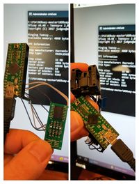
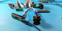
On Board Dumping does not work (it works with VCC pin lifted). To Read/Write the chip in the safest way possible, you will need to desolder the Macronix Flash from the PS4 Mainboard and use a external flasher like the Teensy and SPIway or the Raspberry Pi and JAISPI. For the desoldering part you should use a Hot Air SMD Rework Station like this one and a nozzle to only heat up the pins of the Chip.
Flashing Examples
| ||||||||||||||||||||||||||||||||||||||||||||||||||||||||||||||||||||||||||||||
