CXD90025G: Difference between revisions
mNo edit summary |
mNo edit summary |
||
| Line 5: | Line 5: | ||
<gallery> | <gallery> | ||
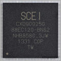
File:CXD90025G - pic01.jpg|CXD90025G - pic01 | File:CXD90025G - pic01.jpg|CXD90025G - pic01 - SCEI and Marvell naming | ||
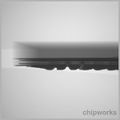
File:CXD90025G - pic02.jpg|CXD90025G - pic02 | File:CXD90025G - pic02.jpg|CXD90025G - pic02 - sideview | ||
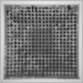
File:CXD90025G - pic03.jpg|CXD90025G - pic03 | File:CXD90025G - pic03.jpg|CXD90025G - pic03 - 20x20 BGA | ||
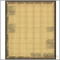
File:CXD90025G - pic04.jpg|CXD90025G - pic04 | File:CXD90025G - pic04.jpg|CXD90025G - pic04 - MRVL inside die detail | ||
File:CXD90025G - pic05.jpg|CXD90025G - pic05 | File:CXD90025G - pic05.jpg|CXD90025G - pic05 - inside die overview | ||
</gallery> | </gallery> | ||
'''Source:''' [http://www.chipworks.com/en/technical-competitive-analysis/resources/blog/inside-the-sony-ps4/ Decapped by Chipworks], see their section on "Network Co-Processor" | '''Source:''' [http://www.chipworks.com/en/technical-competitive-analysis/resources/blog/inside-the-sony-ps4/ Decapped by Chipworks], see their section on "Network Co-Processor" | ||
Revision as of 20:32, 27 January 2014

SCEI CXD90025G
Custom ASIC from Marvell (it even has the 88EC120-BNS2 Marvell naming)
Source: Decapped by Chipworks, see their section on "Network Co-Processor"
Note: It's likely that this chip is way more than simply a "Network Co-Processor"
It is connected to its own DDR3 worker RAM K4B2G1646E-BCK0, the main serial flash MX25L25635FMI-10G and SATA bridge MB86C311B etc. see also File:PS4_-_SAA-001_diagram.png
This secundairy processor was nicknamed MediaCon by the community before any official release because of its role of handling media (online Wireless/GbLAN, Bluray Drive and Harddrive) even in standby. It is not its official name (which is unknown at this moment).
Likely connected to APU by PCI_Express x4 / [HyperTransport] or simular highspeed, low tracecount bus (Marvell ASIC suggests PCI_Express).
| ||||||||||||||||||||||||||||||||||||||||||||||||||||||||||||||||||||||||||||||
