Syscon Hardware: Difference between revisions
mNo edit summary |
Strike Venom (talk | contribs) m (→Retail: see Service Manuals) |
||
| Line 14: | Line 14: | ||
| [[CECHBxx]] || 0x02 || [[COK-00x#COK-001|COK-001]] || [[CXR713120-201GB]] || 0B8E || | | [[CECHBxx]] || 0x02 || [[COK-00x#COK-001|COK-001]] || [[CXR713120-201GB]] || 0B8E || | ||
|- | |- | ||
| [[CECHCxx]] || 0x03 || [[COK-00x#COK-002|COK-002]] || [[CXR713120-201GB]] || 0C16 || | | [[CECHCxx]] || 0x03 || [[COK-00x#COK-002|COK-002]] || [[CXR713120-201GB]]<br /> or<br />[[CXR713120-202GB]] || 0C16 || | ||
|- | |- | ||
| style="text-align:center; background-color:lightgrey;" | <span style="background-color:lightgrey;">[[CECHDxx]]</span> || colspan="6" style="text-align:center; background-color:lightgrey;" | <span style="background-color:lightgrey;">SKU never released</span> | | style="text-align:center; background-color:lightgrey;" | <span style="background-color:lightgrey;">[[CECHDxx]]</span> || colspan="6" style="text-align:center; background-color:lightgrey;" | <span style="background-color:lightgrey;">SKU never released</span> | ||
|- | |- | ||
| [[CECHExx]] || 0x04 || [[COK-00x#COK-002|COK-002]]<br /> or<br />[[COK-00x#COK-002W|COK-002W]] || [[CXR713120-201GB]] || 0C16 || | | [[CECHExx]] || 0x04 || [[COK-00x#COK-002|COK-002]]<br /> or<br />[[COK-00x#COK-002W|COK-002W]] || [[CXR713120-201GB]]<br /> or<br />[[CXR713120-202GB]] || 0C16 || | ||
|- | |- | ||
| style="text-align:center; background-color:lightgrey;" | <span style="background-color:lightgrey;">[[CECHFxx]]</span> || colspan="6" style="text-align:center; background-color:lightgrey;" | <span style="background-color:lightgrey;">SKU never released</span> | | style="text-align:center; background-color:lightgrey;" | <span style="background-color:lightgrey;">[[CECHFxx]]</span> || colspan="6" style="text-align:center; background-color:lightgrey;" | <span style="background-color:lightgrey;">SKU never released</span> | ||
|- | |- | ||
| [[CECHGxx]] || 0x05 || [[SEM-00x|SEM-001]] || [[CXR713120-201GB]] || 0D52 || | | [[CECHGxx]] || 0x05 || [[SEM-00x|SEM-001]] || [[CXR713120-201GB]]<br /> or<br />[[CXR713120-202GB]]<br /> or<br />[[CXR713120-203GB]] || 0D52 || | ||
|- | |- | ||
| [[CECHHxx]] || 0x06 || [[DIA-00x#DIA-001|DIA-001]] || [[CXR714120-301GB]] || 0DBF || | | [[CECHHxx]] || 0x06 || [[DIA-00x#DIA-001|DIA-001]] || [[CXR714120-301GB]] || 0DBF || | ||
| Line 55: | Line 55: | ||
|- | |- | ||
|} | |} | ||
nbsp; | |||
==Prototypes== | ==Prototypes== | ||
Revision as of 18:28, 4 May 2013
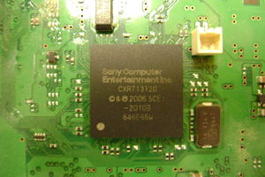
Syscon is the main power controller chip. It is responsible for powering up the various power systems and for configuring and initialising the CELL BE, RSX and South Bridge. It communicates with these devices via seperate SPI busses. There is external access by JTAG (disabled at factory by blowing a fuse), an EEPROM programming interface and Serial (UART). The Syscon is a SoC and consists of an ARM7TDMI (ARMv4) CPU, a 256KB EEPROM and 16KB RAM.
Serialnumbers @ SKU
Retail
nbsp;
Prototypes
| Model | Type | Board | Syscon part no. |
Soft Id. |
Active JTAG | Notes |
|---|---|---|---|---|---|---|
| DECR1000(A/J) | 0x01 | TMU-520 | CXR713F120A | 03FB | ? | |
| DEH-H1000A(S)(-E(S)) | 0x01 | COK-001 (Prototype) | CXR713F120A | 0B67 | ? | |
| DEH-H1001-D | 0x01 | COOKIE-13 | CXR713F120A | ?0B67? | ? |
Not mentioned:
0F29 - ?
0F38 - ?
Syscon Externalised Ports
Note: for more specific information per model, see the links to each subppage in the Serialnumbers @ SKU table.
Syscon UART
| BGA | Name | Description |
|---|---|---|
| P16 | UART0_TxD | Serial Transmit |
| P15 | UART0_RxD | Serial Receive |
You can attach a 3.3v TTL cable (LV-TTL) to the UART on syscon (UART0_TxD, UART0_RxD). Baud rate is 57600. There is a simple plaintext protocol involved. This varies on different syscon models. Example:
<command>:<hash>
Where the hash is the sum of command bytes & 0xFF
you should terminate commands with \r\n, the syscon messages are only terminated with \n
Here are some of the commands/messages encountered:
Messages:
Power applied (standby mode)
OK 00000000:3A

Power on
# (PowerOn State):7F

Power off (Hard shutdown)
# (PowerOff State):DD

After Fan test:
# (PowerOff State) (Fatal):36

No text, invalid hash:
NG F0000002:4D

Commands:
VER:ED
OK 00000000 S1E 00 00 065D:A4

ERRLOG:CB
OK 00000000:3A

DATE:1E
NG F0000003:4E
Syscon (SPI) EEPROM
| BGA | Name | Description |
|---|---|---|
| F16 | CSB | Chip Select (needs always 3.3V ) |
| H16 | DO | Serial Data Output |
| G16 | DI | Serial Data Input |
| E16 | SKB | Serial Data Clock |
| U15 | WCB | Write Protect |
| U16 | RBB | Read Data back (Verify) |
Syscon JTAG
disabled in factory after production on retailmodels
| BGA | Name | Description |
|---|---|---|
| L8 | JRTCK | Return Test Clock |
| K8 | JTCK | Test Clock |
| K9 | JTDO | Test Data Out |
| L9 | JTMS | Test Mode State / Test Mode Select |
| K7 | JTDI | Test Data In |
| L7 | JNTAST | Write Protect |
Syscon Underlaying ports
Syscon Cell SPI Bus
| BGA | Name | Description |
|---|---|---|
| M2 | /BE_SPI_CS | Chip Select |
| N2 | BE_SPI_DO | Serial Data Output |
| M1 | BE_SPI_DI | Serial Data Input |
| N1 | BE_SPI_CLK | Serial Data Clock |
| P2 | /BE_RESET | CellBE Reset |
| P1 | BE_POWGOOD | CellBE PowerGood |
| T2 | /BE_INT | CellBE Interrupt |
Syscon Southbridge SPI Bus
| BGA | Name | Description |
|---|---|---|
| B9 | /SB_SPI_CS | Chip Select |
| B8 | SB_SPI_DO | Serial Data Output |
| A9 | SB_SPI_DI | Serial Data Input |
| A8 | SB_SPI_CLK | Serial Data Clock |
