Template:Syscon pinout BGA 200 pads: Difference between revisions
Jump to navigation
Jump to search
No edit summary |
No edit summary |
||
| Line 195: | Line 195: | ||
| R13 || SW_1_B || Connected to TC7WB66FK (IC5005) pins 3 and 7, and to (IC5006) pin 4, through 1K resistor. The TC7WB66FK chip "duplicates" the MK_I2C_SCL/MK_I2C_SDA bus into a secondary XCG_I2C_SCL/XCG_I2C_SDA bus for the clock reference chip/s<br>+2.5V_LREG_XCG_500_MEM. Analog Voltage for the core PLL of IC5004, Clock Generator used to support the Rambus XDR memory subsystem and Redwood logic interface. | | R13 || SW_1_B || Connected to TC7WB66FK (IC5005) pins 3 and 7, and to (IC5006) pin 4, through 1K resistor. The TC7WB66FK chip "duplicates" the MK_I2C_SCL/MK_I2C_SDA bus into a secondary XCG_I2C_SCL/XCG_I2C_SDA bus for the clock reference chip/s<br>+2.5V_LREG_XCG_500_MEM. Analog Voltage for the core PLL of IC5004, Clock Generator used to support the Rambus XDR memory subsystem and Redwood logic interface. | ||
|- | |- | ||
| T13 || SW_4_B || Connected to 88E6108 ethernet controller (IC3503) pin 94 (signal named P3_ENABLE_PD)<br>Connected to (Q6003) transistor (switches +3.3V_SB_VDDIO)<br>+5V_USB, +1.8V_SB_PERI | | T13 || SW_4_B || Connected to 88E6108 ethernet controller (IC3503) pin 94 (signal named P3_ENABLE_PD)<br>Connected to (Q6003) transistor (switches +3.3V_SB_VDDIO)<br>Connected to [[Regulators#OnSemi_NCP511SN25T1G_.282.5V_150_mA_CMOS_Low_Iq_Low-Dropout_Voltage_Regulator.29 | OnSemi NCP511SN25T1G]] (IC6011) pin 3 (switches +2.5V_SB_PLL_VDDC)<br>+5V_USB, +1.8V_SB_PERI | ||
|- | |- | ||
| R12 || SW_3 || Connected to [[Regulators#Rohm_BD3520FVM-TR_.28Single_channel_Regulator_Driver_IC.29|Rohm BD3520FVM-TR]] (IC6305) pin 3 (switches +1.2V_SB_VDDC and +1.2V_SB_VDDR) | | R12 || SW_3 || Connected to [[Regulators#Rohm_BD3520FVM-TR_.28Single_channel_Regulator_Driver_IC.29|Rohm BD3520FVM-TR]] (IC6305) pin 3 (switches +1.2V_SB_VDDC and +1.2V_SB_VDDR) | ||
Revision as of 07:19, 17 October 2022


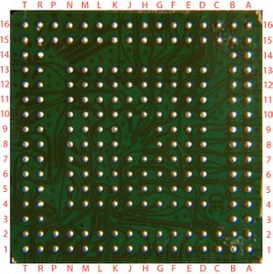
| Pad# | Name | Port | Description |
|---|---|---|---|
| T2 | BE_INT | Port M Cell Control Line |
Connected to CELL 90nm pad AW19 |
| R1 | PM7 | ||
| R2 | PM6 | ||
| P1 | BE_POWGOOD | Connected to CELL 90nm pad AV20 | |
| P2 | BE_RESET | Connected to CELL 90nm pad AW20 | |
| N1 | BE_SPI_CLK | Connected to CELL 90nm pad AY13 (SPI Bus) | |
| N2 | BE_SPI_DO | Connected to CELL 90nm pad AV13 (SPI Bus) | |
| M1 | BE_SPI_DI | Connected to CELL 90nm pad AR13 (SPI Bus) | |
| M2 | BE_SPI_CS | Connected to CELL 90nm pad AP13 (SPI Bus) | |
| L4 | PL8 | Port N | unused |
| L5 | PL7 | ||
| K4 | PL6 | ||
| K5 | PL5 | ||
| J4 | PL4 | ||
| J5 | PL3 | ||
| H4 | PL2 | ||
| H5 | PL1 | ||
| H6 | PL0 | ||
| A8 | SB_SPI_CLK | Port K | Southbridge SPI Bus |
| B8 | SB_SPI_DO | ||
| A9 | SB_SPI_DI | ||
| B9 | SB_SPI_CS | ||
| A10 | DVE_I2C_SCL | Connected to Digital Video Encoder CXM4024R pin 35 | |
| B10 | DVE_I2C_SDA | Connected to Digital Video Encoder CXM4024R pin 36 | |
| A11 | ACDC_STBY | Connected to Power Supply (small connector). This signal enables +12V_MAIN power rail (big prongs) | |
| B11 | PK0 | ||
| B5 | PJ7 | Port J | |
| A5 | DISC_OUT12_SW | ||
| B2 | DISC_OUT8_SW | ||
| A2 | DISC_IN | ||
| B3 | SW_10 | ||
| A3 | SW_0 | Connected to Fujitsu MB39A116PFT (IC6003) pins 9 and 10 (switches +3.3V_MISC and +5V_MISC) Connected to Texas Instruments SN105233DBTR (IC6301) pin 10 (switches +1.7_MISC) | |
| B4 | SW_8_B | Connected to Mitsumi MM1561JFBE (IC2408) pin 5 (switches +1.8V_ANA) Connected to Mitsumi MM1593DFBEG (IC2407) pin 5 (switches +3.3V_ANA) Connected to base pin of DTC144EUA-T106 (Q2401) transistor (switches +5V_ANA ?) +1.5V VDDIO for both AVCG & RSX Analog IO | |
| A4 | SW_8_C | Connected to Texas Instruments SN105233DBTR (IC6301) pin 9 (switches +1.8V_RSX_FBVDDQ) Connected to OnSemi NCP511SN18T1 (IC6008) pin 3 (switches +1.8V_RSX_PLL_VDD) | |
| L16 | SW_PCI | Port I | Connected to Mitsumi MM1591FFBEG pin 5, and Mitsumi MM1593DFBEG pin 5 (switches +1.5V_BRIDGE and +3.3V_BRIDGE) for the PS2 bridge CXD9208GP Connected to PCI service connector pin 80 |
| L15 | DISC_CHUCK | ||
| M16 | DISC_PHOT_LED | ||
| M15 | SW_2 | Connected to Texas Instruments TPS51117PWRG4 (IC6302) pin 1 (switches +1.8V_VDD_MEM) | |
| N16 | DIAG_MODE | ||
| N15 | BACKUP_MODE | ||
| E6 | HDMI_INT | Port H | |
| D6 | VD_CECI0 | ||
| E7 | PH5 | ||
| D7 | RSX_POW_FAIL | Connected to OnSemi NCP5318FTR2G (IC6201) pin 7 | |
| E8 | MUL_CHKSTP_IN | ||
| D8 | MUL_TRG_IN | ||
| E9 | SYS_THR_ALRT | Connected to CELL 90nm pad AP23 | |
| D9 | SB_INT | ||
| M11 | SW_ATA | Port G | Switches +5V_BD and +12V_BD |
| N11 | SW_4_A | Connected to pin 9 of CN3701 connector (wifi board signal named 11G_PWR_EN) Connected to base pin of transistor UMH2NTN (Q3501) who switches IC3502 pin 5, and IC3501 pin 3 (+1.2V_ESW, +1.9V_ESW, +3.3V_ESW for Ethernet Controller) | |
| M10 | XDR_FET_VREF | ||
| N10 | XDR_FET_SCK | ||
| M9 | BUZZER | ||
| N9 | SW_PWM | Unknown output ? (connected to the Switch board) | |
| M8 | FANPWM1 | Secondary fan output (non-retail PS3 models only) | |
| N8 | FANPWM0 | Primary fan output (all PS3 models) | |
| E10 | MUL_CHKSTP_OUT | Port F | |
| D10 | MUL_TAG_OUT | ||
| E11 | SB_CGRESET | ||
| D11 | SB_RESET | Connected to 88SA8040-TBC1 SATA2PATA BluRay controller pin 17 Connected to GL852 (IC3305) USB HUB pin 38 Connected to Multi-card-board connector CN3219 pin 7 | |
| E12 | BT_WAKEON | Connected to pin 30 of CN3701 connector (wifi board signal named BT_WAKE). This is a syscon input | |
| D12 | PF2 BE_VCS_1.25_ON |
COK-001/COK-002 PF2 (Not connected) SEM-001 BE_VCS_1.25_ON | |
| E13 | PF1 BE_VCS_1.30_ON |
COK-001/COK-002 PF1 (Not connected) SEM-001 BE_VCS_1.30_ON | |
| D13 | SW_1_A | Connected to Mitsumi MM1593DFBEG (IC6020) pin 5 (switches +3.3V_MK_VDD) for Clock Synthesizer | |
| A12 | EJECT_SW | Port E | |
| B12 | POW_SW | ||
| A13 | SB_EBUS_RESET | ||
| B13 | SB_EBUS_BRDY | ||
| A14 | PE3 | ||
| B14 | VD_CECI1 | ||
| A15 | BE_POW_FAIL | Connected to OnSemi NCP5318FTR2G (IC6103) pin 7 | |
| B15 | POW_FAIL | ||
| F13 | SW_5_B | Port D | Connected to Rohm BD3520FVM-TR (IC6200) pin 3 (switches +1.2V_RSX_VDDR) |
| F12 | MK_EN | Connected to clock generator ICS1493G-18LFT (IC5001 pin #16 on COK-001, COK-002, SEM-001) | |
| G13 | BEVRM_VID5 | Connected to OnSemi NCP5318FTR2G (IC6103) pin 30 | |
| G12 | BEVRM_VID4 | Connected to OnSemi NCP5318FTR2G (IC6103) pin 3 | |
| H13 | BEVRM_VID3 | Connected to OnSemi NCP5318FTR2G (IC6103) pin 2 | |
| H12 | BEVRM_VID2 | Connected to OnSemi NCP5318FTR2G (IC6103) pin 1 | |
| J13 | BEVRM_VID1 | Connected to OnSemi NCP5318FTR2G (IC6103) pin 32 | |
| J12 | BEVRM_VID0 | Connected to OnSemi NCP5318FTR2G (IC6103) pin 31 | |
| K13 | SW_HDD | Port C | |
| K12 | I2CBUS_EN | Connected to TC7WB66FK pins 3 and 7 (IC5005 on SEM-001) through 1K resistor (in COK-001 the resistor is missing, a.k.a. this syscon line is N/C). This chip "duplicates" the MK_I2C_SCL/MK_I2C_SDA bus into a secondary XCG_I2C_SCL/XCG_I2C_SDA bus for the clock reference chip/s | |
| L13 | RSXVRM_VID5 | Connected to OnSemi NCP5318FTR2G (IC6201) pin 30 | |
| L12 | RSXVRM_VID4 | Connected to OnSemi NCP5318FTR2G (IC6201) pin 3 | |
| M13 | RSXVRM_VID3 | Connected to OnSemi NCP5318FTR2G (IC6201) pin 2 | |
| M12 | RSXVRM_VID2 | Connected to OnSemi NCP5318FTR2G (IC6201) pin 1 | |
| N13 | RSXVRM_VID1 | Connected to OnSemi NCP5318FTR2G (IC6201) pin 32 | |
| N12 | RSXVRM_VID0 | Connected to OnSemi NCP5318FTR2G (IC6201) pin 31 | |
| T15 | SW_8_A | Port B | Connected to Rohm BD3504FVM-TR (IC6304) pin 3 (switches +1.5V_YC_RC_VDDA). Analog voltage supplies, VDD_A |
| R14 | SW_7_A | Connected to OnSemi NCP5318FTR2G (IC6103) pin 29 Connected to Toshiba TC7SG08FU (IC6107) pin 1 (+1.0V_BE_VDDC) Cell BE core voltage supply (VDD) then VCS (the core array voltage). Note, the VID values stored on the CELL itself are not available to be read yet. So the default VID of the VRM is used until then. | |
| T14 | SW_6 | Connected to Rohm BD3520FVM-TR (IC6303) pin 3 (switches +1.2V_YC_RC_VDDIO). I/O voltage supplies, VDD_IO for CELL and RSX | |
| R13 | SW_1_B | Connected to TC7WB66FK (IC5005) pins 3 and 7, and to (IC5006) pin 4, through 1K resistor. The TC7WB66FK chip "duplicates" the MK_I2C_SCL/MK_I2C_SDA bus into a secondary XCG_I2C_SCL/XCG_I2C_SDA bus for the clock reference chip/s +2.5V_LREG_XCG_500_MEM. Analog Voltage for the core PLL of IC5004, Clock Generator used to support the Rambus XDR memory subsystem and Redwood logic interface. | |
| T13 | SW_4_B | Connected to 88E6108 ethernet controller (IC3503) pin 94 (signal named P3_ENABLE_PD) Connected to (Q6003) transistor (switches +3.3V_SB_VDDIO) Connected to OnSemi NCP511SN25T1G (IC6011) pin 3 (switches +2.5V_SB_PLL_VDDC) +5V_USB, +1.8V_SB_PERI | |
| R12 | SW_3 | Connected to Rohm BD3520FVM-TR (IC6305) pin 3 (switches +1.2V_SB_VDDC and +1.2V_SB_VDDR) | |
| T12 | VD_CECO1 | ||
| R11 | VD_CECO0 | ||
| N7 | STBY_LED | Port A | |
| M7 | POW_LED | ||
| N6 | AUDIO_MUTE | Uses a transistor, to switch another 2 transistors, that switches pins AOUTA#18 and AOUTB#15 of Cirrus CS4351-CZZR 192 kHz Stereo DAC (pins 9 and 11 of the MultiAV connector) | |
| M6 | SW_7_B | ||
| N5 | BT_RESET | Connected to pin 10 of CN3701 connector (wifi board signal named SYSCON_RST). This is a syscon output | |
| M5 | GBE_RESET | ||
| N4 | SW_5_A | Connected to OnSemi NCP5318FTR2G (IC6201) pin 29 Connected to Toshiba TC7SG08FU (IC6204) pin 1 (+1.2V_RSX_VDDC) | |
| M4 | SW_9 | ||
| J16 | RBB | EEPROM Interface | |
| K16 | PI7 | ||
| J15 | WCB | ||
| K15 | PI6 | ||
| E16 | SKB | ||
| E15 | PP3 | ||
| G16 | DI | ||
| G15 | PP2 | ||
| H16 | DO | ||
| H15 | PP1 | ||
| F16 | CSB | ||
| F15 | PP0 | ||
| H11 | TESTMODE | Reset & Clock | |
| B16 | OSCOUT | ||
| C16 | OSCIN | ||
| D16 | 32KOUT | ||
| D15 | 32KIN | ||
| T5 | EXTAL | ||
| T4 | XTAL | ||
| T7 | XXTALO | ||
| J11 | RST | ||
| R4 | AVSUO | Power Port | Ground |
| R5 | AVDUO | +3.3V_EVER | |
| G6 | AVSS | Ground | |
| C2 | AVREF2 | Ground | |
| B1 | AVREF1 | +3.3V_EVER | |
| F7 | AVDD | +3.3V_EVER | |
| K11 | VSSF | Ground | |
| K6 | VSSF | Ground | |
| L6 | VDDF | +3.3V_EVER | |
| G7 | VSS | Ground | |
| G8 | |||
| G10 | |||
| T6 | |||
| R6 | |||
| T3 | |||
| L1 | |||
| E1 | |||
| C15 | VSSep | EEPROM Ground | |
| G11 | VDDep | EEPROM Power (+3.3V_EVER) | |
| F11 | VDDbat | +battery | |
| H7 | DVDD | +1.8V_EVER | |
| J10 | |||
| K10 | |||
| L10 | |||
| L11 | |||
| R7 | |||
| J7 | |||
| F8 | VDD3 | +3.3V_EVER | |
| F10 | |||
| H10 | |||
| J6 | |||
| F6 | |||
| D2 | VDD2 | +1.5V_RSX_VDDIO | |
| R3 | VDD1 | +1.2V_MC2_VDDIO | |
| L2 | VDD0 | +1.2V_MC2_VDDIO | |
| A16 | NC | ||
| T16 | |||
| T1 | |||
| A1 | |||
| G9 | |||
| F9 | |||
| L8 | JRTCK | JTAG Interface | |
| K8 | JTCK | ||
| K9 | JTDO | ||
| L9 | JTMS | ||
| K7 | JTDI | ||
| L7 | JNTAST | ||
| A6 | PR3 | Port R | |
| B6 | MC_P_OFF_REQ | ||
| A7 | MC_ALIVE | ||
| B7 | MC_RESERVED1 | ||
| R10 | RMC_IN | Port Q | Connected to missing IR receiver in the Switch boards (IR remote control input using SIRC protocol and SERV_SIRCS) |
| T11 | PQ5 | ||
| T10 | PQ4 | ||
| T8 | THR_I2C_SCL | ||
| T9 | THR_I2C_SDA | ||
| R9 | PQ1 | ||
| R8 | RSX_FBVDD_SEL | Connected to Texas Instruments SN105233DBTR (IC6301) through transistor/s | |
| P16 | UART0_TxD | Port P | Serial Transmit |
| P15 | UART0_RxD | Serial Receive | |
| R16 | HDMI_I2C_SCL | ||
| R15 | HDMI_I2C_SDA | ||
| D1 | MK_I2C_SCL | Port O | Connected to clock generator ICS1493G-18LFT (IC5001 pin #46 on COK-001) |
| C1 | MK_I2C_SDA | Connected to clock generator ICS1493G-18LFT (IC5001 pin #47 on COK-001) | |
| G4 | PO7 | ||
| F4 | HDMI_RST0 | ||
| G5 | PO5 | ||
| F5 | DISC_IN_MECHA | ||
| E4 | EJECT_MECHA | ||
| D4 | XDR_FET_RST | ||
| E5 | GX_VSRST | ||
| D5 | XCG_EN | Connected to ICS9218AGLFT and ICS9214DGLFT pin 11 (IC5002, IC5003 and IC5004 on COK-001 and COK-002). Reference clocks for BE, RSX, SB | |
| K2 | VD_VINT1 | Port N | |
| K1 | VD_VINT0 | ||
| J2 | RSX_INT | ||
| J1 | RSX_FLDO | ||
| H2 | PN6 | ||
| H1 | PN5 | ||
| G2 | RSX_RESET | ||
| G1 | RSX_SPI_CLK | RSX SPI Bus | |
| F2 | RSX_SPI_DO | ||
| F1 | RSX_SPI_DI | ||
| E2 | RSX_SPI_CS | ||