Flash (Hardware): Difference between revisions

From PS3 Developer wiki
Jump to navigation Jump to search
mNo edit summary
Line 28: Line 28:
| 1x [[K8P2716UZC-QI4D|Samsung K8P2716UZC-QI4D]] || {{No}} || {{No}} || {{No}} || {{No}} || - || - || - || - || - || {{Yes}} || {{Yes}} || {{Yes}} ||   
| 1x [[K8P2716UZC-QI4D|Samsung K8P2716UZC-QI4D]] || {{No}} || {{No}} || {{No}} || {{No}} || - || - || - || - || - || {{Yes}} || {{Yes}} || {{Yes}} ||   
|-
|-
| 1x [[MX29GL128ELT2I-90G|Macronix MX29GL128ELT2I-90G]] || {{No}} || {{No}} || {{No}} || {{No}} || - || - || - || {{Yes}} || {{Yes}} || - || - || {{Yes}} ||   
| 1x [[MX29GL128ELT2I-90G|Macronix MX29GL128ELT2I-90G]] || {{No}} || {{No}} || {{No}} || {{No}} || - || - || - || {{Yes}} || {{Yes}} || {{Yes}} || - || {{Yes}} ||   
|-
|-
|}
|}
Line 34: Line 34:
===Non Retail===
===Non Retail===
Reference Tool DECR1000A Communication Processor board :
1x Samsung K9F2G08U0M (NAND 1x2Gbit=256MB total)
1x [[K9F2G08U0M|Samsung K9F2G08U0M]] (NAND 1x2Gbit=256MB total)


== Pinout Flash chips ==
== Other Flash ==


=== NAND ===
=== Renesas HN58X2504TIE (EEPROM) ===
 
==== Samsung K9F1G08U0A-PIB0 or K9F1G08UOB-PIB0 (NAND) ====
 
<div style="float:right">[[File:TOSP1-48pin.png|200px|thumb|left|48-pin TSOP1 Standard Type<br /> 12mm x 20mm<br />Samsung K9F1G08U0A-PIB0]]<br />[[File:Samsung_K9F1G08U0A-PIB0.JPG|200px|thumb|left|One of the 2 Samsung K9F1G08U0A-PIB0 on a NAND based FAT]]</div>
 
Datasheets:
http://www.ps3devwiki.com/files/documents/-%20Datasheets/NAND/
* [http://www.trisaster.de/file/sony/ps3/hardware/K9F1G08U0A.pdf K9F1G08U0A Datasheet]
* [http://www1.futureelectronics.com/doc/SAMSUNG/K9F1G08U0B-PCB0T00.pdf K9F1G08U0B Datasheet]
<pre>productcode meaning:
K - Memory
9 - NAND Flash
F - Small Classification : SLC Normal
1G - Density : 1Gigabit (128MB)
0 - Technology : Normal (x8)
8 - Organisation : x8
U - Vcc Supply Voltage : min 2.7V - Max 3.6V / typ. 3.3V
0 - Mode : Normal
A - Generation : 2nd
-
P - Package : 48pin TSOP1 (12mm x 20mm / 0.5mm pitch)) Lead-free
I - Temperature : Industrial
B - Customer Bad Block : Include Bad Block
0 - PreProgram Version : None</pre>
 
<table><tr><td>
{| border="1" cellspacing="0" cellpadding="5" border="#999" class="wikitable" style="border:1px solid #999; border-collapse: collapse;"
|- bgcolor="#cccccc"
! Pin !! Usage !! Remarks
|-
| 1 || style="color:white; background-color:darkgrey;" | NC || style="color:white; background-color:darkgrey;" | No Connection
|-
| 2 || style="color:white; background-color:darkgrey;" | NC || style="color:white; background-color:darkgrey;" | No Connection
|-
| 3 || style="color:white; background-color:darkgrey;" | NC || style="color:white; background-color:darkgrey;" | No Connection
|-
| 4 || style="color:white; background-color:darkgrey;" | NC || style="color:white; background-color:darkgrey;" | No Connection
|-
| 5 || style="color:white; background-color:darkgrey;" | NC || style="color:white; background-color:darkgrey;" | No Connection
|-
| 6 || style="color:white; background-color:darkgrey;" | NC || style="color:white; background-color:darkgrey;" | No Connection
|-
| 7 || R/B || Read/Busy Output
|-
| 8 || RE || Read Enable
|-
| 9 || CE || Chip Enable
|-
| 10 || style="color:white; background-color:darkgrey;" | NC || style="color:white; background-color:darkgrey;" | No Connection
|-
| 11 || style="color:white; background-color:darkgrey;" | NC || style="color:white; background-color:darkgrey;" | No Connection
|-
| 12 || Vcc || Vcc (min 2.7V-max 3.6V / typ 3.3V)
|-
| 13 || Vss || Ground
|-
| 14 || style="color:white; background-color:darkgrey;" | NC || style="color:white; background-color:darkgrey;" | No Connection
|-
| 15 || style="color:white; background-color:darkgrey;" | NC || style="color:white; background-color:darkgrey;" | No Connection
|-
| 16 || CLE || Command Latch Enable
|-
| 17 || ALE || Address Latch Enable
|-
| 18 || WE || Write Enable
|-
| 19 || WP || Write Protect
|-
| 20 || style="color:white; background-color:darkgrey;" | NC || style="color:white; background-color:darkgrey;" | No Connection
|-
| 21 || style="color:white; background-color:darkgrey;" | NC || style="color:white; background-color:darkgrey;" | No Connection
|-
| 22 || style="color:white; background-color:darkgrey;" | NC || style="color:white; background-color:darkgrey;" | No Connection
|-
| 23 || style="color:white; background-color:darkgrey;" | NC || style="color:white; background-color:darkgrey;" | No Connection
|-
| 24 || style="color:white; background-color:darkgrey;" | NC || style="color:white; background-color:darkgrey;" | No Connection
|-
|}
</td><td>&nbsp;&nbsp;</td><td>
{| border="1" cellspacing="0" cellpadding="5" border="#999" class="wikitable" style="border:1px solid #999; border-collapse: collapse;"
|- bgcolor="#cccccc"
! Pin !! Usage !! Remarks
|-
| 48 || style="color:white; background-color:darkgrey;" | NC || style="color:white; background-color:darkgrey;" | No Connection
|-
| 47 || style="color:white; background-color:darkgrey;" | NC || style="color:white; background-color:darkgrey;" | No Connection
|-
| 46 || style="color:white; background-color:darkgrey;" | NC || style="color:white; background-color:darkgrey;" | No Connection
|-
| 45 || style="color:white; background-color:darkgrey;" | NC || style="color:white; background-color:darkgrey;" | No Connection
|-
| 44 || I/O7 ||
|-
| 43 || I/O6 ||
|-
| 42 || I/O5 ||
|-
| 41 || I/O4 ||
|-
| 40 || style="color:white; background-color:darkgrey;" | NC || style="color:white; background-color:darkgrey;" | No Connection
|-
| 39 || style="color:white; background-color:darkgrey;" | NC || style="color:white; background-color:darkgrey;" | No Connection
|-
| 38 || style="color:white; background-color:darkgrey;" | NC || style="color:white; background-color:darkgrey;" | No Connection
|-
| 37 || Vcc || Vcc (min 2.7V-max 3.6V / typ 3.3V)
|-
| 36 || Vss || Ground
|-
| 35 || style="color:white; background-color:darkgrey;" | NC || style="color:white; background-color:darkgrey;" | No Connection
|-
| 34 || style="color:white; background-color:darkgrey;" | NC || style="color:white; background-color:darkgrey;" | No Connection
|-
| 33 || style="color:white; background-color:darkgrey;" | NC || style="color:white; background-color:darkgrey;" | No Connection
|-
| 32 || I/O3 ||
|-
| 31 || I/O2 ||
|-
| 30 || I/O1 ||
|-
| 29 || I/O0 ||
|-
| 28 || style="color:white; background-color:darkgrey;" | NC || style="color:white; background-color:darkgrey;" | No Connection
|-
| 27 || style="color:white; background-color:darkgrey;" | NC || style="color:white; background-color:darkgrey;" | No Connection
|-
| 26 || style="color:white; background-color:darkgrey;" | NC || style="color:white; background-color:darkgrey;" | No Connection
|-
| 25 || style="color:white; background-color:darkgrey;" | NC || style="color:white; background-color:darkgrey;" | No Connection
|-
|}
</td></tr></table>
 
==== Samsung K9F2G08U0M (NAND) ====
1x 2 Gbit NAND as used on Reference Tool DECR1000A Communication Processor board
 
<div style="float:right">[[File:TSOP1-2Gbit.png|200px|thumb|left|Samsung K9F2G08U0M<br />48-pin TSOP1 Standard Type 12mm x 20mm<br />used on Reference Tool DECR1000A Communication Processor board]]</div>
 
[http://datasheet.semirim.com/ds/view.cgi?file=data/www.samsung.com/Products/Semiconductor/Flash/NAND/2Gbit/K9F2G16U0M/ds_k9f2gxxx0m.pdf.gz Datasheet] / [http://www.ps3devwiki.com/files/documents/-%20Datasheets/NAND/Samsung_K9F2G08U0M.pdf Samsung_K9F2G08U0M.pdf]
 
<pre>productcode meaning:
K - Memory
9 - NAND Flash
F - Small Classification : SLC Normal
2G - Density : 2Gigabit (256MB)
0 - Technology : Normal (x8)
8 - Organisation : x8
U - Vcc Supply Voltage : min 2.7V - Max 3.6V / typ. 3.3V
0 - Mode : Normal
M - Generation :
-
?P - Package : 48pin TSOP1 (12mm x 20mm / 0.5mm pitch)) Lead-free
?I - Temperature : Industrial
?B - Customer Bad Block : Include Bad Block
?0 - PreProgram Version : None</pre>
 
<table><tr><td>
{| border="1" cellspacing="0" cellpadding="5" border="#999" class="wikitable" style="border:1px solid #999; border-collapse: collapse;"
|- bgcolor="#cccccc"
! Pin !! Usage !! Remarks
|-
| 1 || style="color:white; background-color:darkgrey;" | NC || style="color:white; background-color:darkgrey;" | No Connection
|-
| 2 || style="color:white; background-color:darkgrey;" | NC || style="color:white; background-color:darkgrey;" | No Connection
|-
| 3 || style="color:white; background-color:darkgrey;" | NC || style="color:white; background-color:darkgrey;" | No Connection
|-
| 4 || style="color:white; background-color:darkgrey;" | NC || style="color:white; background-color:darkgrey;" | No Connection
|-
| 5 || style="color:white; background-color:darkgrey;" | NC || style="color:white; background-color:darkgrey;" | No Connection
|-
| 6 || style="color:white; background-color:darkgrey;" | NC || style="color:white; background-color:darkgrey;" | No Connection
|-
| 7 || R/B || Read/Busy Output
|-
| 8 || RE || Read Enable
|-
| 9 || CE || Chip Enable
|-
| 10 || style="color:white; background-color:darkgrey;" | NC || style="color:white; background-color:darkgrey;" | No Connection
|-
| 11 || style="color:white; background-color:darkgrey;" | NC || style="color:white; background-color:darkgrey;" | No Connection
|-
| 12 || Vcc || Vcc (min 2.7V-max 3.6V / typ 3.3V)
|-
| 13 || Vss || Ground
|-
| 14 || style="color:white; background-color:darkgrey;" | NC || style="color:white; background-color:darkgrey;" | No Connection
|-
| 15 || style="color:white; background-color:darkgrey;" | NC || style="color:white; background-color:darkgrey;" | No Connection
|-
| 16 || CLE || Command Latch Enable
|-
| 17 || ALE || Address Latch Enable
|-
| 18 || WE || Write Enable
|-
| 19 || WP || Write Protect
|-
| 20 || style="color:white; background-color:darkgrey;" | NC || style="color:white; background-color:darkgrey;" | No Connection
|-
| 21 || style="color:white; background-color:darkgrey;" | NC || style="color:white; background-color:darkgrey;" | No Connection
|-
| 22 || style="color:white; background-color:darkgrey;" | NC || style="color:white; background-color:darkgrey;" | No Connection
|-
| 23 || style="color:white; background-color:darkgrey;" | NC || style="color:white; background-color:darkgrey;" | No Connection
|-
| 24 || style="color:white; background-color:darkgrey;" | NC || style="color:white; background-color:darkgrey;" | No Connection
|-
|}
</td><td>&nbsp;&nbsp;</td><td>
{| border="1" cellspacing="0" cellpadding="5" border="#999" class="wikitable" style="border:1px solid #999; border-collapse: collapse;"
|- bgcolor="#cccccc"
! Pin !! Usage !! Remarks
|-
| 48 || style="color:white; background-color:darkgrey;" | NC || style="color:white; background-color:darkgrey;" | No Connection
|-
| 47 || style="color:white; background-color:darkgrey;" | NC || style="color:white; background-color:darkgrey;" | No Connection
|-
| 46 || style="color:white; background-color:darkgrey;" | NC || style="color:white; background-color:darkgrey;" | No Connection
|-
| 45 || style="color:white; background-color:darkgrey;" | NC || style="color:white; background-color:darkgrey;" | No Connection
|-
| 44 || I/O7 ||
|-
| 43 || I/O6 ||
|-
| 42 || I/O5 ||
|-
| 41 || I/O4 ||
|-
| 40 || style="color:white; background-color:darkgrey;" | NC || style="color:white; background-color:darkgrey;" | No Connection
|-
| 39 || style="color:white; background-color:darkgrey;" | NC || style="color:white; background-color:darkgrey;" | No Connection
|-
| 38 || PRE || Power-On Read Enable<br /><small>PRE controls auto read operation executed during power-on. <br />Power-on auto-read is enabled when PRE pin is tied to VCC.</small>
|-
| 37 || Vcc || Vcc (min 2.7V-max 3.6V / typ 3.3V)
|-
| 36 || Vss || Ground
|-
| 35 || style="color:white; background-color:darkgrey;" | NC || style="color:white; background-color:darkgrey;" | No Connection
|-
| 34 || style="color:white; background-color:darkgrey;" | NC || style="color:white; background-color:darkgrey;" | No Connection
|-
| 33 || style="color:white; background-color:darkgrey;" | NC || style="color:white; background-color:darkgrey;" | No Connection
|-
| 32 || I/O3 ||
|-
| 31 || I/O2 ||
|-
| 30 || I/O1 ||
|-
| 29 || I/O0 ||
|-
| 28 || style="color:white; background-color:darkgrey;" | NC || style="color:white; background-color:darkgrey;" | No Connection
|-
| 27 || style="color:white; background-color:darkgrey;" | NC || style="color:white; background-color:darkgrey;" | No Connection
|-
| 26 || style="color:white; background-color:darkgrey;" | NC || style="color:white; background-color:darkgrey;" | No Connection
|-
| 25 || style="color:white; background-color:darkgrey;" | NC || style="color:white; background-color:darkgrey;" | No Connection
|-
|}
</td></tr></table>
 
=== NOR ===
 
==== Spansion S29GL128N90TFIR2 (NOR) ====
 
<div style="float:right">[[File:S29GLxxxN.png|200px|thumb|left|56-pin TSOP1 Standard Type<br />14mm x 20mm<br />Spansion S29GLxxxN]]</div>
 
[http://www.sltdigital.com/product/product_pdf/sencond_hdx_ic/memory/S29GL256.pdf Datasheet]
 
<pre>productcode meaning:
S29GL128N - 3.0 Volt-only, 512 Megabit (32M x 16-bit/64Mx8-bit), Page-Mode, Flash Memory, 110nm
90 - Speed option : 90ns
T - Package type: TSOP
F - Package materials set : Lead-free
I - Temperature range : Industrial
R2 - ?Vio = 2.7 to 3.6V, lowest address sector protected?</pre>
 
{| border="1" cellspacing="0" cellpadding="5" border="#999" class="wikitable" style="border:1px solid #999; border-collapse: collapse;"
|- bgcolor="#cccccc"
! Pin !! Usage !! Remarks
|-
| 1 || '''A23''' || No Connection for S29GL128N
|-
| 2 || A22 ||
|-
| 3 || A15 ||
|-
| 4 || A14 ||
|-
| 5 || A13 ||
|-
| 6 || A12 ||
|-
| 7 || A11 ||
|-
| 8 || A10 ||
|-
| 9 || A9 ||
|-
| 10 || A8 ||
|-
| 11 || A19 ||
|-
| 12 || A20 ||
|-
| 13 || WE# || Write Enable
|-
| 14 || RESET# || Reset
|-
| 15 || A21 ||
|-
| 16 || '''WP#/ACC''' || '''Write Protect / Accelerated Program Operation'''
|-
| 17 || RD/BY# || Ready/Busy Output
|-
| 18 || A18 ||
|-
| 19 || A17 ||
|-
| 20 || A7 ||
|-
| 21 || A6 ||
|-
| 22 || A5 ||
|-
| 23 || A4 ||
|-
| 24 || A3 ||
|-
| 25 || A2 ||
|-
| 26 || A1 ||
|-
| 27 || style="color:white; background-color:darkgrey;" | NC || style="color:white; background-color:darkgrey;" | No Connection
|-
| 28 || style="color:white; background-color:darkgrey;" | NC || style="color:white; background-color:darkgrey;" | No Connection
|-
|}
{| border="1" cellspacing="0" cellpadding="5" border="#999" class="wikitable" style="border:1px solid #999; border-collapse: collapse;"
|- bgcolor="#cccccc"
! Pin !! Usage !! Remarks
|-
| 29 || Vio || Vio - Output Buffer Power
|-
| 30 || style="color:white; background-color:darkgrey;" | NC || style="color:white; background-color:darkgrey;" | No Connection
|-
| 31 || A0 ||
|-
| 32 || CE# || Chip Enable
|-
| 33 || VSS || Ground
|-
| 34 || OE# || Output Enable
|-
| 35 || DQ0 ||
|-
| 36 || DQ8 ||
|-
| 37 || DQ1 ||
|-
| 38 || DQ9 ||
|-
| 39 || DQ2 ||
|-
| 40 || DQ10 ||
|-
| 41 || DQ3 ||
|-
| 42 || DQ11 ||
|-
| 43 || Vcc || Vcc (min 2.7V-max 3.6V / typ 3.0V)
|-
| 44 || DQ4 ||
|-
| 45 || DQ12 ||
|-
| 46 || DQ5 ||
|-
| 47 || DQ13 ||
|-
| 48 || DQ6 || '''*OTP?'''
|-
| 49 || DQ14 ||
|-
| 50 || DQ7 || '''*OTP?'''
|-
| 51 || DQ15'''/A-1''' ||
|-
| 52 || VSS || Ground
|-
| 53 || '''#BYTE''' || BYTE# Selects 8-bit or 16-bit mode (NC on Samsung K8Q2815UQB-PI4B NOR)
|-
| 54 || A16 ||
|-
| 55 || style="color:white; background-color:darkgrey;" | NC || style="color:white; background-color:darkgrey;" | No Connection
|-
| 56 || A24 || No Connection for S29GL128N and S29GL256N
|-
|}
 
==== Spansion S29GL128P90TFIR2 (NOR) ====
 
<div style="float:right">[[File:S29GLxxxP.png|200px|thumb|left|56-pin TSOP1 Standard Type<br />14mm x 20mm<br />Spansion S29GLxxxP]]</div>
 
[http://www.spansion.com/Support/Datasheets/S29GL-P_00.pdf Datasheet]
 
<pre>productcode meaning:
S29GL128P - 3.0 Volt-only, 512 Megabit (32M x 16-bit/64Mx8-bit), Page-Mode, Flash Memory, 90nm
90 - Speed option : 90ns
T - Package type: TSOP
F - Package materials set : Lead-free
I - Temperature range : Industrial
R2 - ?Vio = 2.7 to 3.6V, lowest address sector protected?</pre>
 
{| border="1" cellspacing="0" cellpadding="5" border="#999" class="wikitable" style="border:1px solid #999; border-collapse: collapse;"
|- bgcolor="#cccccc"
! Pin !! Usage !! Remarks
|-
| 1 || '''A23''' || No Connection for S29GL128P
|-
| 2 || A22 ||
|-
| 3 || A15 ||
|-
| 4 || A14 ||
|-
| 5 || A13 ||
|-
| 6 || A12 ||
|-
| 7 || A11 ||
|-
| 8 || A10 ||
|-
| 9 || A9 ||
|-
| 10 || A8 ||
|-
| 11 || A19 ||
|-
| 12 || A20 ||
|-
| 13 || WE# || Write Enable
|-
| 14 || RESET# || Reset
|-
| 15 || A21 ||
|-
| 16 || WP#/ACC || Write Protect / Accelerated Program Operation
|-
| 17 || RY/BY# || Ready/Busy Output
|-
| 18 || A18 ||
|-
| 19 || A17 ||
|-
| 20 || A7 ||
|-
| 21 || A6 ||
|-
| 22 || A5 ||
|-
| 23 || A4 ||
|-
| 24 || A3 ||
|-
| 25 || A2 ||
|-
| 26 || A1 ||
|-
| 27 || style="color:white; background-color:darkgrey;" | NC || style="color:white; background-color:darkgrey;" | No Connection
|-
| 28 || style="color:white; background-color:darkgrey;" | NC || style="color:white; background-color:darkgrey;" | No Connection
|-
|}
{| border="1" cellspacing="0" cellpadding="5" border="#999" class="wikitable" style="border:1px solid #999; border-collapse: collapse;"
|- bgcolor="#cccccc"
! Pin !! Usage !! Remarks
|-
| 29 || Vio || Vio - Output Buffer Power
|-
| 30 || style="color:white; background-color:darkgrey;" | NC || style="color:white; background-color:darkgrey;" | No Connection
|-
| 31 || A0 ||
|-
| 32 || CE# || Chip Enable
|-
| 33 || VSS || Ground
|-
| 34 || OE# || Output Enable
|-
| 35 || DQ0 ||
|-
| 36 || DQ8 ||
|-
| 37 || DQ1 ||
|-
| 38 || DQ9 ||
|-
| 39 || DQ2 ||
|-
| 40 || DQ10 ||
|-
| 41 || DQ3 ||
|-
| 42 || DQ11 ||
|-
| 43 || Vcc || Vcc (min 2.7V-max 3.6V / typ 3.0V)
|-
| 44 || DQ4 ||
|-
| 45 || DQ12 ||
|-
| 46 || DQ5 ||
|-
| 47 || DQ13 ||
|-
| 48 || DQ6 || '''*OTP?'''
|-
| 49 || DQ14 ||
|-
| 50 || DQ7 || '''*OTP?'''
|-
| 51 || DQ15'''/A-1''' ||
|-
| 52 || VSS || Ground
|-
| 53 || '''#BYTE''' || BYTE# Selects 8-bit or 16-bit mode (NC on Samsung K8Q2815UQB-PI4B NOR)
|-
| 54 || A16 ||
|-
| 55 || style="color:white; background-color:darkgrey;" | A25 || style="color:white; background-color:darkgrey;" | No Connection for S29GL128P, S29GL256P and S29GL512P
|-
| 56 || A24 || No Connection for S29GL128P and S29GL256P
|-
|}
 
==== Samsung K8Q2815UQB-PI4B (NOR) ====
 
<div style="float:right">[[File:TOSP1-56pin.png|200px|thumb|left|56-pin TSOP1 Standard Type<br />14mm x 20mm]]<br />[[File:Samsung K8Q2815UQB-PI4B (NOR).jpg|200px|thumb|left|Samsung K8Q2815UQB-PI4B (NOR) as seen on modern PS3 Slim]]</div>
 
[http://www.samsung.com/global/system/business/semiconductor/product/2007/8/7/144546ds_k8q2815uqb_rev11.pdf Datasheet]
 
<pre>productcode meaning:
K - Memory
8 - NOR Flash
Q - Small Classification : Page Mode DDP
28 - Density : 128M, 8M / 16Bank / 8^8
15 - Dual Bank Boot Block (Bank1, Bank2) : 16M, 2M / 14M
U - Vcc : 3.0V / 3.3V (2.7V~3.6V)
Q - Device Type: Top and Bottom Boot Block
B - Generation : 3rd Generation
-
P - Package : TSOP1 (Lead Free)
I - Temp : Industrial
4B - Speed : 60ns/25ns (Page)</pre>
 
=====NOTE=====
Multiple Bank architectures (8 banks)
- Bank 0 : 8Mbit (4Kw x 8 and 32Kw x 15)
- Bank 1 :24Mbit (32Kw x 48)
- Bank 2 : 24Mbit (32Kw x 48)
- Bank 3 : 8Mbit (4Kw x 8 and 32Kw x 15)
- Bank 4 : 8Mbit (4Kw x 8 and 32Kw x 15)
- Bank 5 :24Mbit (32Kw x 48)
- Bank 6 : 24Mbit (32Kw x 48)
- Bank 7 : 8Mbit (4Kw x 8 and 32Kw x 15)
OTP Block : Extra 256 word
- 128word for factory and 128word for customer OTP (only on first Virtual Chip, A22=low)
 
{| border="1" cellspacing="0" cellpadding="5" border="#999" class="wikitable" style="border:1px solid #999; border-collapse: collapse;"
|- bgcolor="#cccccc"
! Pin !! Usage !! Remarks
|-
| 1 || style="color:white; background-color:darkgrey;" | NC || style="color:white; background-color:darkgrey;" | No Connection
|-
| 2 || A22 || Virtual Chip Enable of 2nd Chip
|-
| 3 || A15 ||
|-
| 4 || A14 ||
|-
| 5 || A13 ||
|-
| 6 || A12 ||
|-
| 7 || A11 ||
|-
| 8 || A10 ||
|-
| 9 || A9 ||
|-
| 10 || A8 ||
|-
| 11 || A19 ||
|-
| 12 || A20 ||
|-
| 13 || WE || Write Enable
|-
| 14 || RESET || Reset
|-
| 15 || A21 ||
|-
| 16 || WP/ACC || Write Protect / Accelerated Program Operation
|-
| 17 || RD/BY || Ready/Busy Output
|-
| 18 || A18 ||
|-
| 19 || A17 ||
|-
| 20 || A7 ||
|-
| 21 || A6 ||
|-
| 22 || A5 ||
|-
| 23 || A4 ||
|-
| 24 || A3 ||
|-
| 25 || A2 ||
|-
| 26 || A1 ||
|-
| 27 || style="color:white; background-color:darkgrey;" | NC || style="color:white; background-color:darkgrey;" | No Connection
|-
| 28 || style="color:white; background-color:darkgrey;" | NC || style="color:white; background-color:darkgrey;" | No Connection
|-
|}
{| border="1" cellspacing="0" cellpadding="5" border="#999" class="wikitable" style="border:1px solid #999; border-collapse: collapse;"
|- bgcolor="#cccccc"
! Pin !! Usage !! Remarks
|-
| 29 || VCCQ || VccQ
|-
| 30 || style="color:white; background-color:darkgrey;" | NC || style="color:white; background-color:darkgrey;" | No Connection
|-
| 31 || A0 ||
|-
| 32 || CE || Chip Enable
|-
| 33 || VSS || Ground
|-
| 34 || OE || Output Enable
|-
| 35 || DQ0 ||
|-
| 36 || DQ8 ||
|-
| 37 || DQ1 ||
|-
| 38 || DQ9 ||
|-
| 39 || DQ2 ||
|-
| 40 || DQ10 ||
|-
| 41 || DQ3 ||
|-
| 42 || DQ11 ||
|-
| 43 || Vcc || Vcc (min 2.7V-max 3.6V / typ 3.0V)
|-
| 44 || DQ4 ||
|-
| 45 || DQ12 ||
|-
| 46 || DQ5 ||
|-
| 47 || DQ13 ||
|-
| 48 || DQ6 || *OTP?
|-
| 49 || DQ14 ||
|-
| 50 || DQ7 || *OTP?
|-
| 51 || DQ15 ||
|-
| 52 || VSS || Ground
|-
| 53 || style="color:white; background-color:darkgrey;" | NC || style="color:white; background-color:darkgrey;" | No Connection
|-
| 54 || A16 ||
|-
| 55 || style="color:white; background-color:darkgrey;" | NC || style="color:white; background-color:darkgrey;" | No Connection
|-
| 56 || style="color:white; background-color:darkgrey;" | NC || style="color:white; background-color:darkgrey;" | No Connection
|-
|}
 
*OTP Block Region : 256-word Flash memory region. The data DQ6=1 for customer locked and DQ7=1 for factory locked
 
==== Samsung K8P2716UZC-QI4D (NOR) ====
<div style="float:right">[[File:54TSOP1-Samsung K8P2716UZC-QI4D.png|200px|thumb|left|56-pin TSOP1 Standard Type<br />14mm x 20mm<br />as used for Samsung K8P2716UZC-QI4D]]<br />[[File:K8P2716UZC-QI40.jpg|200px|thumb|left|Samsung K8P2716UZC-QI4D as seen on some JSD-001 boards]]</div>
 
[http://www.samsung.com/global/system/business/semiconductor/product/2010/11/26/478704ds_k8p2716uzc_rev10.pdf Datasheet]
 
<pre>productcode meaning:
K - Memory
8 - NOR Flash
P
27 - Density : 128M x8/x16
18 - Dual Bank Boot Block :
U - Vcc : 3.0V / 3.3V (2.7V~3.6V)
Z - Device Type:
C - Generation : 4rd Generation
-
Q - Package : 56TSOP1
I - Temp : Industrial
4D - Speed : 70ns/30ns(Page)</pre>
 
 
{| border="1" cellspacing="0" cellpadding="5" border="#999" class="wikitable" style="border:1px solid #999; border-collapse: collapse;"
|- bgcolor="#cccccc"
! Pin !! Usage !! Remarks
|-
| 1 || style="color:white; background-color:darkgrey;" | NC || style="color:white; background-color:darkgrey;" | No Connection
|-
| 2 || A22 ||
|-
| 3 || A15 ||
|-
| 4 || A14 ||
|-
| 5 || A13 ||
|-
| 6 || A12 ||
|-
| 7 || A11 ||
|-
| 8 || A10 ||
|-
| 9 || A9 ||
|-
| 10 || A8 ||
|-
| 11 || A19 ||
|-
| 12 || A20 ||
|-
| 13 || WE# || Write Enable
|-
| 14 || RESET# || Reset
|-
| 15 || A21 ||
|-
| 16 || WP#/ACC || Write Protect / Accelerated Program Operation
|-
| 17 || RD/BY# || Ready/Busy Output
|-
| 18 || A18 ||
|-
| 19 || A17 ||
|-
| 20 || A7 ||
|-
| 21 || A6 ||
|-
| 22 || A5 ||
|-
| 23 || A4 ||
|-
| 24 || A3 ||
|-
| 25 || A2 ||
|-
| 26 || A1 ||
|-
| 27 || style="color:white; background-color:darkgrey;" | NC || style="color:white; background-color:darkgrey;" | No Connection
|-
| 28 || style="color:white; background-color:darkgrey;" | NC || style="color:white; background-color:darkgrey;" | No Connection
|-
|}
{| border="1" cellspacing="0" cellpadding="5" border="#999" class="wikitable" style="border:1px solid #999; border-collapse: collapse;"
|- bgcolor="#cccccc"
! Pin !! Usage !! Remarks
|-
| 29 || Vio || Vio - Output Buffer Power
|-
| 30 || style="color:white; background-color:darkgrey;" | NC || style="color:white; background-color:darkgrey;" | No Connection
|-
| 31 || A0 ||
|-
| 32 || CE# || Chip Enable
|-
| 33 || VSS || Ground
|-
| 34 || OE# || Output Enable
|-
| 35 || DQ0 ||
|-
| 36 || DQ8 ||
|-
| 37 || DQ1 ||
|-
| 38 || DQ9 ||
|-
| 39 || DQ2 ||
|-
| 40 || DQ10 ||
|-
| 41 || DQ3 ||
|-
| 42 || DQ11 ||
|-
| 43 || Vcc || Vcc (min 2.7V-max 3.6V / typ 3.0V)
|-
| 44 || DQ4 ||
|-
| 45 || DQ12 ||
|-
| 46 || DQ5 ||
|-
| 47 || DQ13 ||
|-
| 48 || DQ6 ||
|-
| 49 || DQ14 ||
|-
| 50 || DQ7 ||
|-
| 51 || DQ15'''/A-1''' ||
|-
| 52 || VSS || Ground
|-
| 53 || '''#BYTE''' || BYTE# Selects 8-bit or 16-bit mode
|-
| 54 || A16 ||
|-
| 55 || style="color:white; background-color:darkgrey;" | NC || style="color:white; background-color:darkgrey;" | No Connection
|-
| 56 || style="color:white; background-color:darkgrey;" | NC || style="color:white; background-color:darkgrey;" | No Connection
|-
|}
 
 
==== Macronix MX29GL128ELT2I-90G (NOR) ====
 
<div style="float:right">[[File:TOSP1-56pin.png|200px|thumb|left|56-pin TSOP1 Standard Type<br />14mm x 20mm]]<br />[[File:Macronix MX29GL128ELT2I-90G (NOR Flash).jpg|200px|thumb|left|Macronix MX29GL128ELT2I-90G (NOR) as seen on CECH-30.. according to some sources]]</div>
 
[http://www.mxic.com.tw/QuickPlace/hq/PageLibrary4825740B00298A3B.nsf/h_Index/DBACA1C90564EBB248257639003A563A/$File/MX29GL128E,%203V,%20128Mb,%20v1.1.pdf Datasheet]
 
<pre>productcode meaning:
MX29GL Series
3V
128 Mb
16M x 8/8M x 16
90ns
Parallel Flash
TSOP-56
</pre>
 
{| border="1" cellspacing="0" cellpadding="5" border="#999" class="wikitable" style="border:1px solid #999; border-collapse: collapse;"
|- bgcolor="#cccccc"
! Pin !! Usage !! Remarks
|-
| 1 || style="color:white; background-color:darkgrey;" | NC || style="color:white; background-color:darkgrey;" | No Connection
|-
| 2 || A22 ||
|-
| 3 || A15 ||
|-
| 4 || A14 ||
|-
| 5 || A13 ||
|-
| 6 || A12 ||
|-
| 7 || A11 ||
|-
| 8 || A10 ||
|-
| 9 || A9 ||
|-
| 10 || A8 ||
|-
| 11 || A19 ||
|-
| 12 || A20 ||
|-
| 13 || WE# || Write Enable
|-
| 14 || RESET# || Reset
|-
| 15 || A21 ||
|-
| 16 || WP#/ACC || Write Protect / Accelerated Program Operation
|-
| 17 || RD/BY# || Ready/Busy Output
|-
| 18 || A18 ||
|-
| 19 || A17 ||
|-
| 20 || A7 ||
|-
| 21 || A6 ||
|-
| 22 || A5 ||
|-
| 23 || A4 ||
|-
| 24 || A3 ||
|-
| 25 || A2 ||
|-
| 26 || A1 ||
|-
| 27 || style="color:white; background-color:darkgrey;" | NC || style="color:white; background-color:darkgrey;" | No Connection
|-
| 28 || style="color:white; background-color:darkgrey;" | NC || style="color:white; background-color:darkgrey;" | No Connection
|-
|}
{| border="1" cellspacing="0" cellpadding="5" border="#999" class="wikitable" style="border:1px solid #999; border-collapse: collapse;"
|- bgcolor="#cccccc"
! Pin !! Usage !! Remarks
|-
| 29 || VI/O || Vcc I/O (min 2.7V-max 3.6V / typ 3.0V)
|-
| 30 || style="color:white; background-color:darkgrey;" | NC || style="color:white; background-color:darkgrey;" | No Connection
|-
| 31 || A0 ||
|-
| 32 || CE# || Chip Enable
|-
| 33 || GND || Ground
|-
| 34 || OE# || Output Enable
|-
| 35 || Q0 ||
|-
| 36 || Q8 ||
|-
| 37 || Q1 ||
|-
| 38 || Q9 ||
|-
| 39 || Q2 ||
|-
| 40 || Q10 ||
|-
| 41 || Q3 ||
|-
| 42 || Q11 ||
|-
| 43 || Vcc || Vcc (min 2.7V-max 3.6V / typ 3.0V)
|-
| 44 || Q4 ||
|-
| 45 || Q12 ||
|-
| 46 || Q5 ||
|-
| 47 || Q13 ||
|-
| 48 || Q6 ||
|-
| 49 || Q14 ||
|-
| 50 || Q7 ||
|-
| 51 || Q15/A-1 || Q15 (Word Mode) / LSB addr (Byte Mode)
|-
| 52 || GND || Ground
|-
| 53 || BYTE# || Selects 8bits or 16bits mode
|-
| 54 || A16 ||
|-
| 55 || style="color:white; background-color:darkgrey;" | NC || style="color:white; background-color:darkgrey;" | No Connection
|-
| 56 || style="color:white; background-color:darkgrey;" | NC || style="color:white; background-color:darkgrey;" | No Connection
|-
|}
 
=== Pinout Other ===
 
==== Renesas HN58X2504TIE (EEPROM) ====
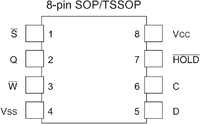
<div style="float:right">[[File:TSSOP-8pin-HN58X2504TIE.png|200px|thumb|left|8-pin TSSOP<br />Renesas HN58X2504TIE]]</div>
Note: although [http://www.edepot.com/playstation3.html#Super_Secrets edepot&others] lists it on the board, I can only find this IC in the sixaxis. <br />
Line 1,079: Line 91:
|-
|-
|}
|}
{{Console}}
[[Category:Flash (Hardware)]]

Revision as of 18:14, 30 March 2012

Flash

The PS3 uses a NOR interface from the South Bridge to address the main firmware flash. On NAND based consoles, it uses the Starship2 as an interleaving bridge chip to the two NAND flash, while on NOR based consoles the single NOR flash is connected directly to the South Bridge.

SKU Differentiation

For a difference between models, see SKU Models

Retail

Flash FAT SLIM Notes
CECHA
CECHB
CECHC
CECHE
CECHE CECHG CECHH CECHK CECHL
CECHM
CECHP
CECHQ
CECH-20xx CECH-21xx CECH-25xx CECH-25xx CECH-30xx
COK
001
COK
002
COK
002W
SEM
001
DIA
001
DIA
002
VER
001
DYN
001
SUR
001
JTP
001
JSD
001
KTE
001
NAND 2x Samsung K9F1G08U0A-PIB0 Yes Yes - - No No No No No No No No
2x Samsung K9F1G08U0B-PIB0 - - - Yes No No No No No No No No
NOR 1x Spansion S29GL128N90TFIR2 No No No No Yes Yes Yes Yes - - - -
1x Samsung K8Q2815UQB-PI4B No No No No - - Yes Yes Yes - - -
1x Spansion S29GL128P90TFIR2 No No No No - - Yes Yes Yes Yes Yes Yes
1x Samsung K8P2716UZC-QI4D No No No No - - - - - Yes Yes Yes
1x Macronix MX29GL128ELT2I-90G No No No No - - - Yes Yes Yes - Yes

Non Retail

Reference Tool DECR1000A Communication Processor board : 1x Samsung K9F2G08U0M (NAND 1x2Gbit=256MB total)

Other Flash

Renesas HN58X2504TIE (EEPROM)

8-pin TSSOP
Renesas HN58X2504TIE

Note: although edepot&others lists it on the board, I can only find this IC in the sixaxis.
Datasheet

productcode meaning:
H - 
N - 
5 -
8 - Organisation : x8bit
X - 
2 - 
5 - 
0 - 
4 - Density : 4-kbit (512x8bit)
T - Package : 8pin plastic TSSOP (TTP-8DAV)
I - Temp : Industrial (-40 to +85 °C 
E - Environment : Lead Free


Each PS3 has a special EEPROM chip on the motherboard using a SPI Serial Interface Renasas chip.

Type Size Speed Voltage Packaging Manufacturer Serial Number Description
EEPROM 4-kbit (512x8bit) 3MHz 1.8V to 5.5V 8-pin TSSOP Renesas HN58X2504TIE PS3 EEPROM chip


Pin Usage Remarks
1 S Chip Select
2 Q Serial data output
3 W Write Protect
4 VSS Ground
5 D Serial data input
6 C Serial Clock
7 HOLD Hold
8 VCC Vcc (min 1.8V-max 5.5V)


Template:Console