Talk:Service Connectors
Jump to navigation
Jump to search
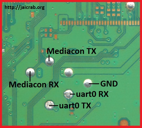
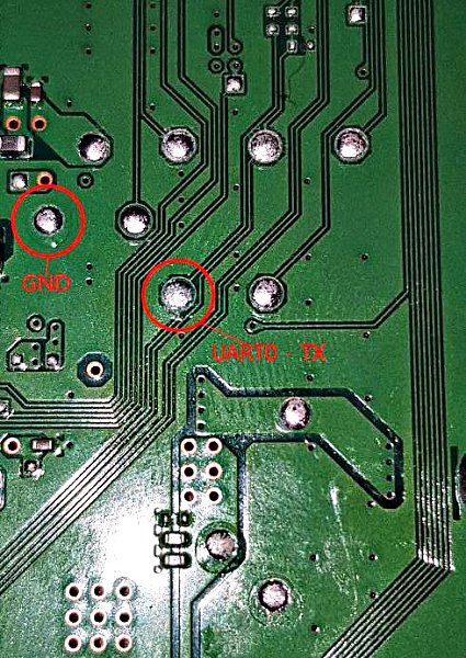
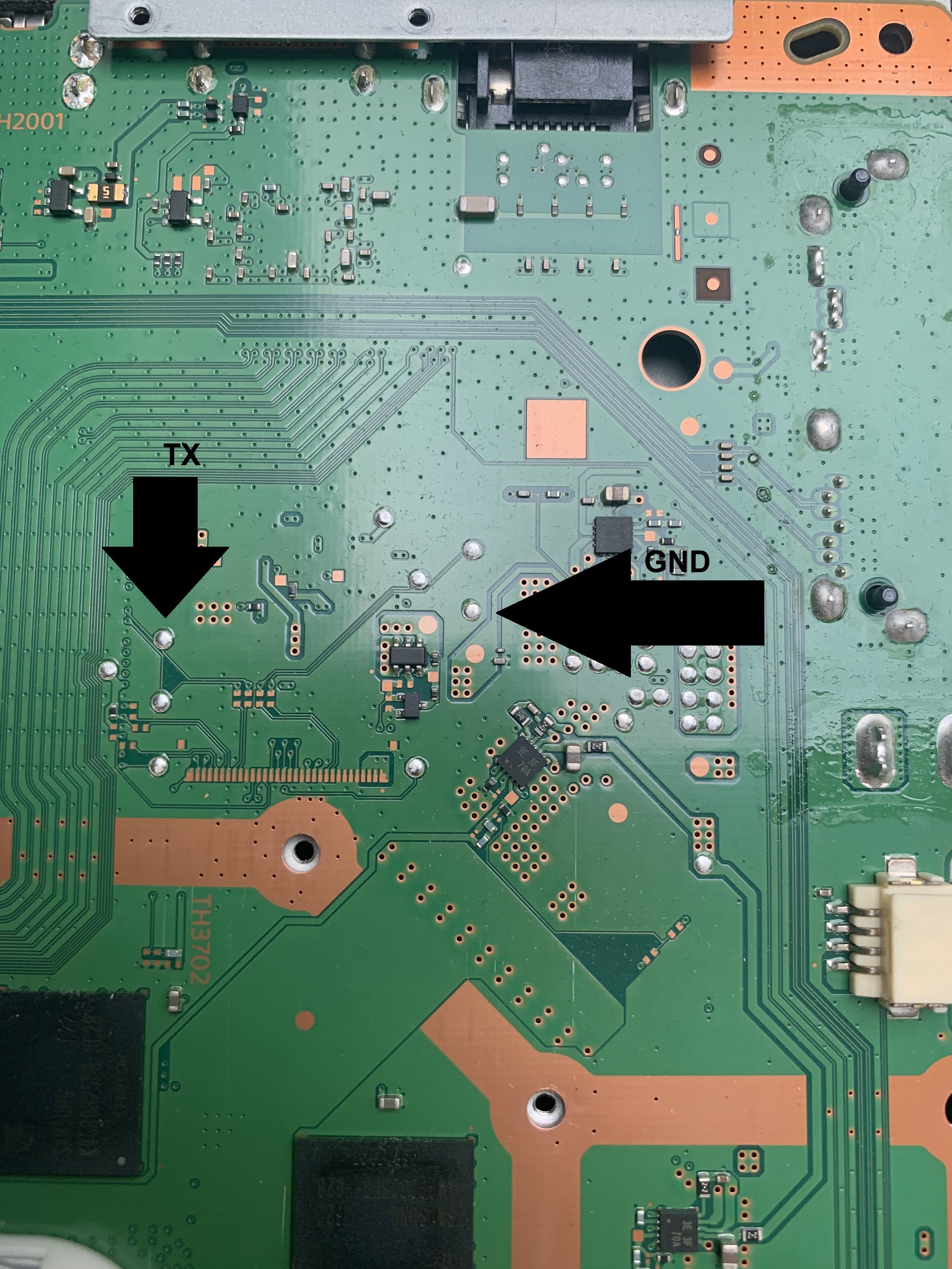
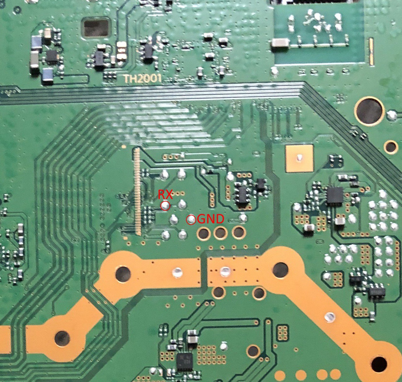
UART Testpoints[edit source]
SAA-001[edit source]
SAC-001[edit source]
SAD-001[edit source]
SAE-004[edit source]
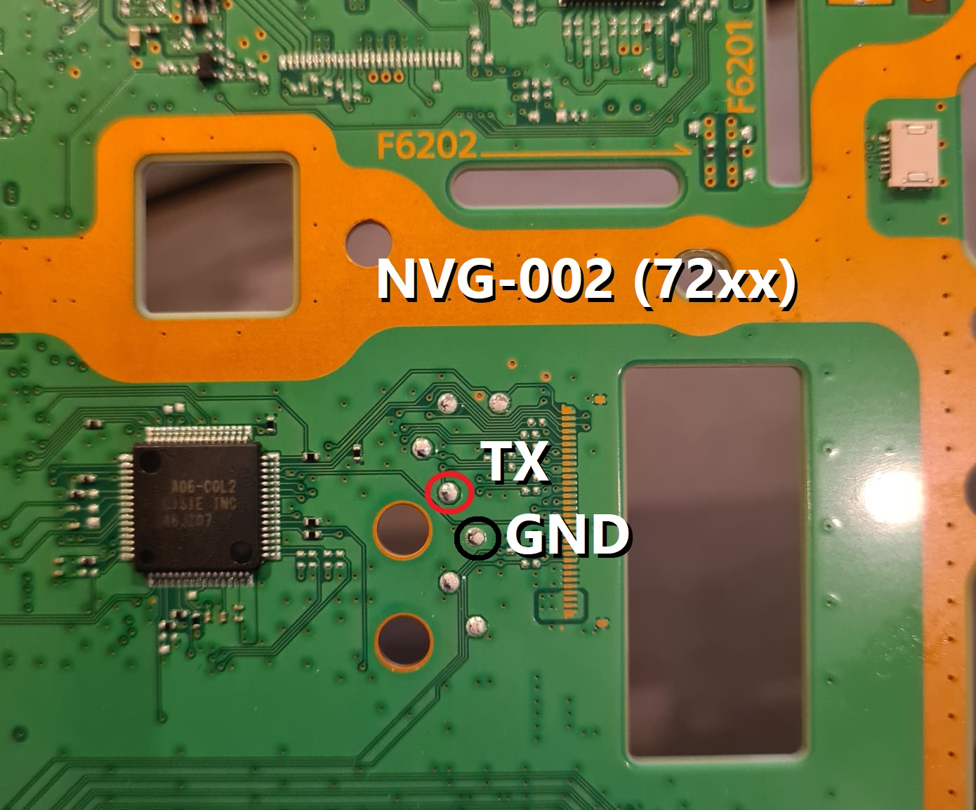
NVG-002[edit source]
Pad Info[edit source]
This pad is used for the same purpose as on the PS3 System; a ZIF connector is preset on prototype versions.
- it looks as if ribbon connectors could easily be soldered onto those pads, seeing as the ground pads are conducive of such.
- yep, that's precisely what they're for (take a look at https://twitter.com/MinaRalwasser/status/1035581527076294656/photo/1 for the ps3 service connector example)
- But what can ultimately be achieved? Aren't there also some points where a USB TTL device could be soldered to?
- You can end up dumping the syscon flash (on ps4 and possibly vita and and ps3 as well) by glitching it
- Dumping and modifying is a big jump though.
- You can also program it (the pinouts are known)
- It would be nice to be able to modify it to skip any error checking (thus be able to boot even with hardware/software issues) - I think the syscon handles this...
1st GEN Pinouts[edit source]
SC
syscon, rl78/g13
  1     P142
  2     P141        VR-VRDY1
  3     P140        VR-VRDY2
  4     P120        power switch(USBHUB)
  5     P47         VR-VRHOT_ICRIT
  6     P46         power switch(BUZZER)
  7     P45         NC
  8     P44         VR-PWROK + APU-PWROK
  9     P43         APU-RESET#
 10     P42         (HDR-A SPI-CS)
 11     P41         power switch(PSU-7)
 12     P40         TOOL0 -> HDR-A pin 22 (open circuit between pin and header)
 13     RESET#      -> HDR-A pin 24
 14     P124        pulldown?
 15     P123        power switch(PSU-5)
 16     P137        testpoint?
 17     P122        -> HDR-A pin 28 (4bit input-only, port 12)
 18     P121        -> HDR-A pin 29 (4bit input-only, port 12)
 19     REGC        cap to GND
 20     Vss         GND
 21     EVss0       GND
 22     Vdd         Vcc
 23     EVdd0       == pin 22
 24     P60         APU i2c dev 0xba
 25     P61         APU i2c dev 0xba
 26     P62         APU i2c dev 0x78/0x98
 27     P63         APU i2c dev 0x78/0x98
 28     P31         FAN-CTL
 29     P64         power switch(HDMI-0 + APU-4)
 30     P65         LED
 31     P66         LED
 32     P67         LED
 33     P77         pulldown
 34     P76
 35     P75         APU?
 36     P74
 37     P73         power switch(USBBRIDGE + HDD)
 38     P72         -> HDR-A pin 12 (HDR-A SPI-SO)
 39     P71         (HDR-A SPI-SI)
 40     P70         -> HDR-A pin 10 (HDR-A SPI-CLK)
 41     P06         power switch(PSU-1)
 42     P05
 43     EVss1       GND
 44     P80         STM8-PWR pin 7 (NRST)
 45     P81         NC testpoint
 46     P82         LED
 47     P83         power switch(PSU-4)
 48     P84         pulldown?
 49     P85         power switch(PSU-2)
 50     P86         power switch(APU-0) + PSW-APU-3 pin 3
 51     P87         VR-EN + power switch(APU-1)
 52     P30         NC testpoint
 53     EVdd1       Vcc
 54     P50         power switch(SB-1 + SB-2 + DDR3)
 55     P51         power switch(SB-0) (6pin near wifi + 8pin between SC/SB)
 56     P52         testpoint?
 57     P53         VR-SM_CLK
 58     P54         VR-SM_DIO
 59     P55         power switch(APU-2)
 60     P56
 61     P57
 62     P17
 63     P16         SB-TP0 looks like SB -> SC interrupt line (INTP5)
 64     P15         SB-TP1 (SPI-CLK)
 65     P14         SB-TP2 (SPI-SI) + SC-P11 in a weird way? + elsewhere
 66     P13         SB-TP3 (SPI-SO)
 67     P12         -> HDR-A pin 15 (SC ucmd UART)
 68     P11         -> HDR-A pin 16 (SC ucmd UART)
 69     P10         SB-TP4 (SPI-CS)
 70     P101        power switch(VR)
 71     P110
 72     P111
 73     P146        NC
 74     P147        power switch(HDMI-1)
 75     P100        power switch(PSU-0)
 76     P156        pulldown?
 77     P155        pulldown?
 78     P154        PSW-APU-2 pin 1 + PSW-APU-3 pin 1
 79     P153        -> HDR-G pin 11
 80     P152        -> HDR-G pin 15
 81     P151        power switch(PSU-3)
 82     P150        WIFI reset?
 83     P27         NC testpoint
 84     P26         STM8-PWR pin 1 + HDR-C pin 8 (POWER#) (serial clock)
 85     P25         STM8-EJECT pin 1 + HDR-C pin 7 (EJECT#)
 86     P24         pulldown?
 87     P23         pulldown?
 88     P22
 89     P21         NC testpoint
 90     P20
 91     P130        power switch(PSU-6) (P130 is tied to sc-internal RESET)
 92     P102
 93     P04         i2c (pcie clockgen smbus?)
 94     P03         -> HDR-F pin 1 (i2c (pcie clockgen smbus?))
 95     P02         -> HDR-F pin 2 (XXX did i fuckup the HDR-F mapping here?)
 96     P01
 97     P00
 98     P145
 99     P144
100     P143

VR (IR3585, 48pin QFN)
Dual Output Digital Multi-Phase Controller
outputs:
    loop 1: VddNb
    loop 2: Vdd
pinout seems to match https://www.infineon.com/dgdl/pb-ir3565a.pdf?fileId=5546d462533600a40153568011cc28e5
  1     RCSP
  2     RCSM
  3     VRDY2               SC-P140
  4     CFP                 NC
  5     VSEN                VddNb sense
  6     VRTN                VddNb sense
  7     RRES
  8     TSEN1               VddNb
  9     V18A
 10     PWRGD/VRDY1         SC-P141
 11     PWROK/EN_L2/INMODE  SC-P44
 12     VINSEN
 13     NC
 14     VIDDIO/SV_ADDR
 15     SVT/SV_ALERT
 16     SV_CLK/VIDSEL1
 17     SV_DIO/VIDSEL0
 18     VRHOT_ICRIT         SC-P47
 19     EN                  SC-P87 + power switch(APU-1)
 20     ADDR_PROT           pulldown
 21     SM_ALERT            pullup
 22     SM_DIO              SC-P54
 23     SM_CLK              SC-P53
 24     NC
 25     VGD/TSEN2/VAUXSEN   Vdd
 26     PWM1                VddNb
 27     PWM2                VddNb
 28     PWM3                VddNb
 29     PWM4                VddNb
 30     PWM2_L2             Vdd
 31     PWM1_L2             Vdd
 32     VRTN_L2             Vdd sense
 33     VSEN_L2             Vdd sense
 34     VCC
 35     RCSM_L2             Vdd
 36     RCSP_L2             Vdd
 37     ISEN1_L2            Vdd
 38     IRTN1_L2            Vdd
 39     ISEN2_L2            Vdd
 40     IRTN2_L2            Vdd
 41     ISEN4               VddNb
 42     IRTN4               VddNb
 43     ISEN3               VddNb
 44     IRTN3               VddNb
 45     ISEN2               VddNb
 46     IRTN2               VddNb
 47     ISEN1               VddNb
 48     IRTN1               VddNb

HDR-A (bottom, 1x30 near sata edge connector)
  1     Vcc?
  2     NC
  3     == pin 1
  4
  5
  6     GND
  7     -> HDR-D pin 2
  8
  9     GND
 10     SC-P70
 11
 12     SC-P72
 13
 14     GND
 15     SC-P12
 16     SC-P11
 17     SC-P51
 18     GND
 19     -> SB?
 20     -> SB?
 21     -> SB?
 22     SC-P40 (TOOL0) open circuit
 23     GND
 24     SC-RESET#
 25     GND
 26     UNK-26
 27     UNK-27
 28     SC-P122
 29     SC-P121
 30     NC

HDR-B (bottom, 1x20 between HDR-A and SB)
  1     Vcc?
  2     GND
  3
  4     GND
  5
  6
  7
  8
  9
 10
 11     GND
 12     SB-20/S (SDIO?) probably for eMMC
 13     GND
 14     SB-19/R (SDIO?)
 15     SB SDIO?
 16     SB SDIO?
 17     SB SDIO?
 18     SB SDIO?
 19     GND
 20     NC

HDR-C (bottom, 2x5 on edge near BD sata connector)
numbering in U-shape
  1     Vcc?
  2     STM8-PWR pin 7 (NRST)
  3     STM8-PWR pin 27 (BEEP)
  4     GND
  5     GND
  6     NC
  7     STM8-PWR pin 1 + SC-P25 (open circuit)
  8     STM8-EJECT pin 1 + SC-P26 (goes thru HDR-G pin 10) (open circuit)
  9     NC
 10     GND

HDR-D (bottom, 2x4 underneath battery)
numbering in U-shape
  1     -> HDR-A pin 8
  2     -> HDR-A pin 7
  3     NC
  4     GND
  5     Vcc?
  6     == pin 5
  7     == pin 5
  8     == pin 5

HDR-E (bottom, 1x14 SB/eth phy related?)
  1     GND
  2     GND
  3
  4     GND
  5
  6     GND
  7
  8     GND
  9
 10
 11     Vcc?
 12     == pin 11
 13     == pin 11
 14     == pin 11

HDR-F (top, near WIFI antennas)
IDT6V41265 smbus
numbering in U-shape
  1     -> IDT6V41265 pin 23 + SC-P03 (DAT)
  2     -> IDT6V41265 pin 22 + SC-P02 (CLK @ 100khz)
  3     NC
  4     GND
  5     Vcc? (connected to some IDT6V41265 voltage pins)
  6     == pin 5
  7     GND
  8     == pin 5

IDT6V41265
clk3 used by SB during ROM (directly out of reset)
clk4 used by SB in late boot
SC (or SB?) writes to smbus while SB ROM is reading IPL
  1     GND
  2     vref?
  3     clk0_0
  4     clk0_1
  5     vref?
  6     GND
  7     vref?
  8     vref?
  9     GND
 10     clk1_0
 11     clk1_1
 12     vref?
 13     vref?
 14     clk2_0
 15     clk2_1
 16     GND
 17     vref?
 18     vref?
 19     NC (testpoint)
 20     NC (testpoint)
 21     GND
 22     smbus CLK 100khz
 23     smbus DAT
 24     reset# (-> SB?)
 25     GND
 26     25mhz xtal
 27     25mhz xtal
 28     vref?
 29     vref?
 30     GND
 31     clk3_0  100mhz SS
 32     clk3_1
 33     vref?
 34     vref?
 35     clk4    100mhz
 36     GND
 37     -> eth phy (clk?)
 38     vref?
 39     vref?
 40     NC (testpoint)
 41
 42     GND
 43
 44
 45     -> hdmi (clk?)
 46     vref?
 47     vref?
 48     GND

HDR-G (top, 1x24 connector to BD)
  1     GND
  2     SATA
  3     SATA
  4     GND
  5     GND
  6     SATA
  7     SATA
  8     GND
  9     GND
 10     -> HDR-C pin 8
 11     SC-P153
 12
 13     STM8-PWR pin 7 (NRST)
 14     GND
 15     SC-P152
 16     hard to track, SB?
 17
 18
 19
 20     GND
 21     STM8-PWR pin 3 (SPI MOSI)
 22     STM8-PWR pin 2 (SPI MISO)
 23     testpoint -> BD?
 24     cap to Vcc?
- Thx F0F
