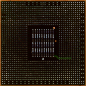
Template:CELL pad layout 65nm
Jump to navigation
Jump to search
| Name | ||||
|---|---|---|---|---|
| Internal | External | |||
| AV13 | SPI_SI/BE_SPI_DO | Connected to Syscon pad N2 (BGA 200 pads layout), or pin 80 (LQFP 128 pins layout) | ||
| AV23 | THERMAL_OVERLOAD/SYS_THR_ALRT | Connected to Syscon pad E9 (BGA 200 pads layout), or pin UNK (LQFP 128 pins layout) through transistor | ||
| AW13 | SPI_EN/BE_SPI_CS | Connected to Syscon pad M2 (BGA 200 pads layout), or pin 83 (LQFP 128 pins layout) | ||
| AW18 | HARD_RESET/BE_RESET_AND | Connected to Syscon pad P2 (BGA 200 pads layout), or pin UNK (LQFP 128 pins layout) | ||
| AY13 | SPI_CLK/BE_SPI_CLK | Connected to Syscon pad N1 (BGA 200 pads layout), or pin 82 (LQFP 128 pins layout) | ||
| BA13 | SPI_SO/BE_SPI_DI | Connected to Syscon pad M1 (BGA 200 pads layout), or pin 81 (LQFP 128 pins layout) through 47 resistor | ||
| BA17 | ATTENTION/BE_INT | Connected to Syscon pad T2 (BGA 200 pads layout), or pin 3 (LQFP 128 pins layout) | ||
| BA19 | POWER_GOOD/BE_POWGOOD | Connected to Syscon pad P1 (BGA 200 pads layout), or pin UNK (LQFP 128 pins layout) | ||
