Template:CELL pad layout 65nm: Difference between revisions
Jump to navigation
Jump to search
(Added photo by deadend) |
No edit summary |
||
| Line 4: | Line 4: | ||
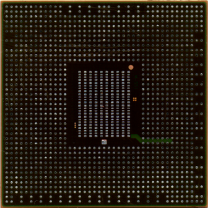
</includeonly><div style="float:right">[[File:Cell_65nm_(1200_dpi_scan).bmp|300px|thumb|left|CELL 65nm pad layout (CELL view)<br>Pad A1 at top-left corner]]</div> | </includeonly><div style="float:right">[[File:Cell_65nm_(1200_dpi_scan).bmp|300px|thumb|left|CELL 65nm pad layout (CELL view)<br>Pad A1 at top-left corner]]</div> | ||
<div style="overflow:auto; <includeonly>height:1200px;</includeonly>"> | |||
{| class="wikitable mw-datatable sortable" style="width:100%; line-height:1em; font-size:0.9em" | {| class="wikitable mw-datatable sortable" style="width:100%; line-height:1em; font-size:0.9em" | ||
|+ {{captionlinks|CELL pad layout 65nm}} | |+ {{captionlinks|CELL pad layout 65nm}} | ||
Revision as of 02:13, 10 November 2022
| Pad | Name | Description |
|---|---|---|
| AV13 | SPI_SI/BE_SPI_DO | < Connected to Syscon pad N2 (BGA 200 pads layout), or pin 80 (LQFP 128 pins layout) |
| AV23 | THERMAL_OVERLOAD/SYS_THR_ALRT | > Connected to Syscon pad E9 (BGA 200 pads layout), or pin UNK (LQFP 128 pins layout) through transistor |
| AW13 | SPI_EN/BE_SPI_CS | < Connected to Syscon pad M2 (BGA 200 pads layout), or pin 83 (LQFP 128 pins layout) |
| AW18 | HARD_RESET/BE_RESET_AND | < Connected to Syscon pad P2 (BGA 200 pads layout), or pin UNK (LQFP 128 pins layout) |
| AY13 | SPI_CLK/BE_SPI_CLK | < Connected to Syscon pad N1 (BGA 200 pads layout), or pin 82 (LQFP 128 pins layout) |
| BA13 | SPI_SO/BE_SPI_DI | > Connected to Syscon pad M1 (BGA 200 pads layout), or pin 81 (LQFP 128 pins layout) through 47 resistor |
| BA17 | ATTENTION/BE_INT | > Connected to Syscon pad T2 (BGA 200 pads layout), or pin 3 (LQFP 128 pins layout) |
| BA19 | POWER_GOOD/BE_POWGOOD | < Connected to Syscon pad P1 (BGA 200 pads layout), or pin UNK (LQFP 128 pins layout) |
