Talk:Regulators: Difference between revisions
Jump to navigation
Jump to search
m (feel free to edit the tables if someone does further research, probably i made some mistakes when trying to meassure onboard SMD components, my purpose was mostlly to see the syscon connections and voltage rails) |
m (→JSD-001 motherboard: syscon voltage control lines official names speculation) |
||
| Line 1: | Line 1: | ||
{{wikify}} | {{wikify}} | ||
==JSD-001 motherboard== | ==JSD-001 motherboard== | ||
All the components listed are controlled by [[Syscon_Hardware|Syscon]] and connected to it by a pin/trace either directlly or indirectlly | All the components listed are controlled by [[Syscon_Hardware|Syscon]] and connected to it by a pin/trace either directlly or indirectlly, the traces are hidden in internal layers of the motherboard | ||
By looking at the first syscon model used by the PS3 [[CXR713120-201GB]] where we know the names of the pin signals it seems these syscon control lines for voltage regulators could be the syscon pins named SW_xx_xx (switches, used as a generic name) | |||
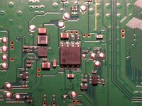
==== Mitsumi 463A (voltage regulator) ==== | ==== Mitsumi 463A (voltage regulator) ==== | ||
<div style="float:right">[[File:Mitsumi 463A.jpg|200px|thumb|left|Mitsumi voltage regulator 463A<br />Seen on a JSD-001 motherboard]]</div> | <div style="float:right">[[File:Mitsumi 463A.jpg|200px|thumb|left|Mitsumi voltage regulator 463A<br />Seen on a JSD-001 motherboard]]</div> | ||
Revision as of 19:25, 4 August 2015
| This article is marked for rewrite/restructuring in proper wiki format. You can help PS3 Developer wiki by editing it. |
JSD-001 motherboard
All the components listed are controlled by Syscon and connected to it by a pin/trace either directlly or indirectlly, the traces are hidden in internal layers of the motherboard
By looking at the first syscon model used by the PS3 CXR713120-201GB where we know the names of the pin signals it seems these syscon control lines for voltage regulators could be the syscon pins named SW_xx_xx (switches, used as a generic name)
Mitsumi 463A (voltage regulator)
| Pin | Signal | Description |
|---|---|---|
| 1 | 5V_EVER | From power supply 5v standby rail (pin 1 of connector CN101) |
| 2 | 3.3V_EVER_B | 3.3v_standby_rail_2 |
| 3 | ? | Goes under package to the black 100 ohm resistor at its right, and from there to syscon SWx-x pin 26 |
| 4 | ? | Goes under package to squared testpad/sinkhole at its right (not connected ?) |
| 5 | V ? | To a capacitor, and from there to ground |
| 6 | ? | To squared testpad/sinkhole at its top (not connected ?) |
| 7 | GND | Ground |
| 8 | 3.3V_EVER_A | 3.3v_standby_rail_1 |
Mitsumi 348A (voltage regulator)
| Pin | Signal | Description |
|---|---|---|
| 1 | ? | Not connected ? |
| 2 | ? | Connected to syscon SWx-x pin 119 |
| 3 | GND | Ground |
| 4 | ? | output voltage rail 1 ?. Connected to pin 100 (and other 10 pins more) of HDMI controller. It has a testpad at the other side |
| 5 | ? | output voltage rail 2 for A/V controller and optical ? (not tested). It has a testpad at the other side |
| 6 | GND | Ground |
| 7 | ? | Connected to syscon SWx-x pin 119 |
| 8 | 5V_EVER | From power supply 5v standby rail (pin 1 of connector CN101) |
Mitsumi 040 810X (close to RSX)
| Pin | Signal | Description |
|---|---|---|
| 1 | ? | connected to 4x sinkholes (it has a testpad at the other side) |
| 2 | ? | hidden under package |
| 3 | GND | Ground |
| 4 | ? | |
| 5 | ? | Connected to syscon SWx-x pin 75 |
| 6 | ? | hidden under package |
| 7 | ? | hidden under package |
| 8 | ? | connected to 2x sinkholes |
D35653 0S25
Next to NOR, on top of the board JSD-001, responsible of the NOR VCC
| Pin | Signal | Description |
|---|---|---|
| 1 | V_OUT | capacitor and 180 ohm resistor to ground... then to 4 sinkholes and at the other side NOR VCC 3.3v (testpoint) |
| 2 | GROUND | |
| 3 | GROUND | |
| 4 | ? | capacitor to ground |
| 5 | ? | Dissapears in a sinkhole and emerges near syscon, connected to SWx-x pin 50 |
| 6 | GROUND | |
| 7 | GROUND | |
| 8 | V_IN_1 | connected to BD9684 pins 3,8,17 |
BD3525
| Pin | Signal | Description |
|---|---|---|
| 1 | V_OUT_x ? | to 4 sinkholes... at the other side to electrolitic capacitor 2.5v 330 |
| 2 | ||
| 3 | ||
| 4 | ||
| 5 | ||
| 6 | ||
| 7 | ? | diode to ground, and capacitor to ground, and diode to 55.8 ohm resistor to pin 1 |
| 8 | ? | capacitor to ground |
| 9 | GROUND | |
| 10 | GROUND | |
| 11 | V_IN_1 | connected to BD9684 pins 3,8,17 |
| 12 | ? | 46Kohm resistor to ground, and a trace that dissapears in a sinkhole and emerges near syscon, connected to SWx-x pin 52 |
| 13 | ? | |
| 14 | V_IN_2 | 0.400mf capacitor to ground, to 4 sinkholes connected to BD3527 (near usb) pins 14 up to 20 and BD3527 (near flash) pins 14 up to 20 |
| 15 | ||
| 16 | ||
| 17 | ||
| 18 | ||
| 19 | ||
| 20 |
BD3527
There are 2 BD3527 on JSD-001 motherboard, one near flash and the other near usb connectors
near flash
| Pin | Signal | Description |
|---|---|---|
| 1 | V_OUT_x ? | to 3 smd components to gnd, to electrolitic capacitor 2.5v 330, to 3 sinkholes with a testpoint at the other side |
| 2 | ||
| 3 | ||
| 4 | ||
| 5 | ||
| 6 | ||
| 7 | ? | capacitor and 1600 ohm resistor to pin 1 |
| 8 | ? | diode ? to ground |
| 9 | GROUND | |
| 10 | GROUND | |
| 11 | V_IN_1 | connected to BD9684 pins 3,8,17 |
| 12 | ? | dissapears in a sinkhole (resistor 23Kohm to ground in the other side) and emerges near syscon, connected to SWx-x pin 95 |
| 13 | ? | dissapears in a sinkhole (capacitor 915nf to ground in the other side) |
| 14 | V_IN_2 | to 3 sinkholes missing at the other side, to 4 sinkholes connected to BD3525 pins 14 up to 20 |
| 15 | ||
| 16 | ||
| 17 | ||
| 18 | ||
| 19 | ||
| 20 |
near usb
| Pin | Signal | Description |
|---|---|---|
| 1 | V_OUT_x ? | 88 ohm resistor to ground, to a testpoint, to 4 sinkholes and to the other side to electrolitic capacitor 2.5v 330 (very close to a ram chip) |
| 2 | ||
| 3 | ||
| 4 | ||
| 5 | ||
| 6 | ||
| 7 | ? | capacitor and 1600 ohm resistor to pin 1 |
| 8 | ? | diode ? to ground |
| 9 | GROUND | |
| 10 | GROUND | |
| 11 | V_IN_1 | connected to BD9684 pins 3,8,17 |
| 12 | ? | 42k ohm resistor to ground, and to a sinkhole that dissapears in the other side and emerges near syscon, connected to SWx-x pin 92 |
| 13 | ? | 1000nf capacitor to ground |
| 14 | V_IN_2 | capacitor to ground, to 4 sinkholes missing in the other side, connected to BD3525 pins 14 up to 20 |
| 15 | ||
| 16 | ||
| 17 | ||
| 18 | ||
| 19 | ||
| 20 |
BD9684 0906
| Pin | Signal | Description |
|---|---|---|
| 1 | ? | sealed coil... then to 8 sinkholes... to BD controller, etc... |
| 2 | ? | dissapears under package |
| 3 | V_? | 0.400mf capacitor to ground... then to 4 sinkholes... at the other side conneced to fuse/thermistor TH7601 |
| 4 | ? | to a sinkhole... at the other side 3.3K resistor to ground, then connected to pins 2 and 3 of a dual transistor (base of TR1, and collector of TR2) |
| 5 | GROUND | |
| 6 | GROUND | |
| 7 | dissapears under package | |
| 8 | V_? | 0.400mf capacitor to ground... then to the same 4 sinkholes of pin 3 |
| 9 | ? | dissapears under package |
| 10 | ? | sealed coil... then tied to pin 11 |
| 11 | ? | to 6 sinkholes... at the other side to unpopulated service connector... etc... |
| 12 | ? | tied to pin 13... capacitor to ground, to a 4x-sinkhole... then to BD controller |
| 13 | ? | tied to pin 12... capacitor to ground, to a 4x-sinkhole... then to BD controller |
| 14 | GROUND | |
| 15 | ? | to a sinkhole... at the other side to BD controller |
| 16 | ? | dissapears under package |
| 17 | V_? | 0.400mf capacitor to ground... then to a sinkhole and tied to pin 3 |
| 18 | ? | towards blu ray laser connector |
| 19 | ? | tied to pin 1 |
| 20 | ? | to a sinkhole... then to pin 6 of the same dual transistor (collector of TR1) |
- pin 5 of the dual transistor (base of TR2) is connected to a long trace that dies in a sinkhole and emerges under syscon, connected to SWx-x pin 42
- the emitter pins of the dual transistor (1 and 4) are connected to a common ground

