Hardware flashing: Difference between revisions
mNo edit summary |
|||
| Line 17: | Line 17: | ||
Because the tristate pin is not connected to the [http://www.ps3devwiki.com/index.php?title=Flash_%28Hardware%29#NOR NOR flash] TSOP package, but to the [[South Bridge]] BGA package, this makes tracing the pin quite difficult. One should be able to locate it by having the running you could ground out the unknown pins whilst checking the continuity of a known address or data line against ground. These should enter high-impedance or no-continuity when you ground out SB_DISABLE. | Because the tristate pin is not connected to the [http://www.ps3devwiki.com/index.php?title=Flash_%28Hardware%29#NOR NOR flash] TSOP package, but to the [[South Bridge]] BGA package, this makes tracing the pin quite difficult. One should be able to locate it by having the running you could ground out the unknown pins whilst checking the continuity of a known address or data line against ground. These should enter high-impedance or no-continuity when you ground out SB_DISABLE. | ||
== Connecting to flasher == | |||
<div style="float:right">[[File:Progskeet.png|200px|thumb|left|Progskeet NAND/NOR flasher board, based on Actel MCU, see http://progskeet.com/)]]</div> | |||
<div style="height:420px; overflow:auto"> | |||
{| border="1" cellspacing="0" cellpadding="5" border="#999" class="wikitable sortable" style="border:1px solid #999; border-collapse: collapse;" | |||
|- bgcolor="#cccccc" | |||
! PAD !! [http://www.progskeet.com/download.php Progskeet] !! Teensy2.0++ | |||
|- | |||
| A0 || adr0 || | |||
|- | |||
| A1 || adr1 || | |||
|- | |||
| A2 || adr2 || | |||
|- | |||
| A3 || adr3 || | |||
|- | |||
| A4 || adr4 || | |||
|- | |||
| A5 || adr5 || | |||
|- | |||
| A6 || adr6 || | |||
|- | |||
| A7 || adr7 || | |||
|- | |||
| A8 || adr8 || | |||
|- | |||
| A9 || adr9 || | |||
|- | |||
| A10 || adr10 || | |||
|- | |||
| A11 || adr11 || | |||
|- | |||
| A12 || adr12 || | |||
|- | |||
| A13 || adr13 || | |||
|- | |||
| A14 || adr14 || | |||
|- | |||
| A15 || adr15 || | |||
|- | |||
| A16 || adr16 || | |||
|- | |||
| A17 || adr17 || | |||
|- | |||
| A18 || adr18 || | |||
|- | |||
| A19 || adr19 || | |||
|- | |||
| A20 || adr20 || | |||
|- | |||
| A21 || adr21 || | |||
|- | |||
| A22 || adr22 || | |||
|- | |||
| DQ0 || dq0 || | |||
|- | |||
| DQ1 || dq1 || | |||
|- | |||
| DQ2 || dq2 || | |||
|- | |||
| DQ3 || dq3 || | |||
|- | |||
| DQ4 || dq4 || | |||
|- | |||
| DQ5 || dq5 || | |||
|- | |||
| DQ6 || dq6 || | |||
|- | |||
| DQ7 || dq7 || | |||
|- | |||
| DQ8 || dq8 || | |||
|- | |||
| DQ9 || dq9 || | |||
|- | |||
| DQ10 || dq10 || | |||
|- | |||
| DQ11 || dq11 || | |||
|- | |||
| DQ12 || dq12 || | |||
|- | |||
| DQ13 || dq13 || | |||
|- | |||
| DQ14 || dq14 || | |||
|- | |||
| DQ15 || dq15 || | |||
|- | |||
| #WE || we || | |||
|- | |||
| CE# || gp0 || | |||
|- | |||
| RST || gp1 || | |||
|- | |||
| TRI || gp2 || | |||
|- | |||
| WP# || gp3 || | |||
|- | |||
| OE# || oe || | |||
|- | |||
| RYBY || rdy || | |||
|- | |||
| VSS || GND || | |||
|- | |||
|} | |||
</div> | |||
= Board Revisions = | = Board Revisions = | ||
Revision as of 08:47, 31 July 2011

Both early launch consoles which feature NAND flash memory and later consoles which feature NOR flash memory are able to be flashed. Currently the preferred method of flashing the dual-NAND consoles is by using an infectus modchip or similar.
Marcan has made a NOR flasher / address sniffer for his PS3 slim by re-purposing a FPGA board made for Wii hacking. noralizer is a git repo that contains the HDL (verilog) and associated host computer tools for flashing/sniffing. There are ~50 signals to solder. Some PS3s contain two NAND flashes (block devices, that interleave their data unlike NOR flash).
Work is currently underway to brink a low cost AVR based NOR flasher that is capable of reading and writing on all consoles by defyboy.
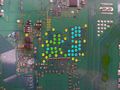
NOR Interface Testpoints
Probably to aid in factory programming, Sony provides NOR testpoints on the bottomside of the motherboard. There are 16 data lines (Word access) and generally 23 Address lines. You will also need to control Chip Enable (#CE), Write Enable (#WE), Tristate (SB_DISABLE) and for some boards Write Protect (#WP)
Tristate
Tristate, or as it is referred to in the service manuals SB_DISABLE exists solely for the purpose of placing the South Bridge pins into high-impedance (the third state) so that we can access the flash without the South Bridge interfering.
Because the tristate pin is not connected to the NOR flash TSOP package, but to the South Bridge BGA package, this makes tracing the pin quite difficult. One should be able to locate it by having the running you could ground out the unknown pins whilst checking the continuity of a known address or data line against ground. These should enter high-impedance or no-continuity when you ground out SB_DISABLE.
Connecting to flasher

| PAD | Progskeet | Teensy2.0++ |
|---|---|---|
| A0 | adr0 | |
| A1 | adr1 | |
| A2 | adr2 | |
| A3 | adr3 | |
| A4 | adr4 | |
| A5 | adr5 | |
| A6 | adr6 | |
| A7 | adr7 | |
| A8 | adr8 | |
| A9 | adr9 | |
| A10 | adr10 | |
| A11 | adr11 | |
| A12 | adr12 | |
| A13 | adr13 | |
| A14 | adr14 | |
| A15 | adr15 | |
| A16 | adr16 | |
| A17 | adr17 | |
| A18 | adr18 | |
| A19 | adr19 | |
| A20 | adr20 | |
| A21 | adr21 | |
| A22 | adr22 | |
| DQ0 | dq0 | |
| DQ1 | dq1 | |
| DQ2 | dq2 | |
| DQ3 | dq3 | |
| DQ4 | dq4 | |
| DQ5 | dq5 | |
| DQ6 | dq6 | |
| DQ7 | dq7 | |
| DQ8 | dq8 | |
| DQ9 | dq9 | |
| DQ10 | dq10 | |
| DQ11 | dq11 | |
| DQ12 | dq12 | |
| DQ13 | dq13 | |
| DQ14 | dq14 | |
| DQ15 | dq15 | |
| #WE | we | |
| CE# | gp0 | |
| RST | gp1 | |
| TRI | gp2 | |
| WP# | gp3 | |
| OE# | oe | |
| RYBY | rdy | |
| VSS | GND |
Board Revisions
COK-001, COK-002, SEM-001
These are the earliest revisions of the PS3 motherboard (CECHA, CECHB, CECHC, CECHE, CECHG) and contain 2 x Samsung K9F1G08U0A-PIB0 128MB NAND Chips for a total of 256MB. These chips are interleaved which is controlled by a proprietary controller chip codenamed "Starship2" or SS2. This chip handles the interleaving and presents the NANDS to the South Bridge as a single large coherent NOR Chip.
DIA-001, DIA-002
These boards were the first to get the NOR flash memory from the middle revisions of the PS3 (CECHH, CECHJ, CECHK). Only a single Spansion S29GL128N90TFIR2 16MB NOR flash chip is used and the Starship2 chip has been completely removed. The 128N is JEDEC CFI compliant and organized as 8,388,608 words or 16,777,216 bytes, addressable as 16-bit words (PS3 modus operandi) and 8-bit / 1 byte when the BYTE# signal is logic zero.
VER-001
Used in the last revisions of the fatter model PS3 (CECHL, CECHM, CECHP, CECHQ), again with the single Spansion S29GL128N90TFIR2 16MB NOR flash with the exception of the CECHL which used a Samsung K8Q2815UQB-P14B 16MB NOR flash.
JSD-001
This is the pinout originally supplied by Marcan for a CECH-2504A, Points match those taken from a CECH-2504B slim console. Most slims may carry this arrangement.
Pinout Gallery
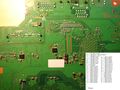
SS2 NOR Testpoints
- VER-001 NOR.JPG
VER-001 NOR Testpoints
DIA-001 NOR Testpoints
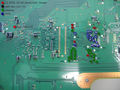
DYN-001 Testpoints
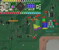
JSD-001 Testpoints
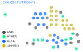
COK-001 NOR Testpoints (only overlay)
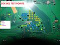
COK-001 NOR Testpoints


