Flash (Hardware): Difference between revisions
Jump to navigation
Jump to search
mNo edit summary |
|||
| Line 2: | Line 2: | ||
= Differentiation = | = Differentiation = | ||
CECHA- | CECHA/COK-00A up to including CECHE/COK-002W : | ||
2x Samsung K9F1G08U0A-PIB0 (2x1Gbit=256MB total) | 2x Samsung K9F1G08U0A-PIB0 (NAND 2x1Gbit=256MB total) | ||
CECHG/SEM-001 : | |||
1x Spansion | 2x Samsung K9F1G08UOB-PIB0 (NAND 2x1Gbit=256MB total) | ||
1x Samsung K8Q2815UQB-PI4B | CECHH/DIA-001 up to including CECHK/DIA-002 : | ||
1x Spansion S29GL128N90TFIR2 (NOR 16MB) | |||
CECHL/VER-001 : | |||
1x Spansion S29GL128P90TFIR2 (NOR 16MB) | |||
CECHL/VER-001 and PS3 Slims : | |||
1x Samsung K8Q2815UQB-PI4B (NOR 16MB) | |||
For a difference between models, see [[SKU Models]] | For a difference between models, see [[SKU Models]] | ||
| Line 14: | Line 21: | ||
==Samsung K9F1G08U0A-PIB0== | ==Samsung K9F1G08U0A-PIB0 or K9F1G08UOB-PIB0 == | ||
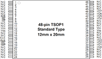
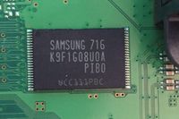
<div style="float:right">[[File:TOSP1-48pin.png|200px|thumb|left|48-pin TSOP1 Standard Type<br /> 12mm x 20mm<br />Samsung K9F1G08U0A-PIB0]]<br />[[File:Samsung_K9F1G08U0A-PIB0.JPG|200px|thumb|left|One of the 2 Samsung K9F1G08U0A-PIB0 on a NAND based FAT]]</div> | <div style="float:right">[[File:TOSP1-48pin.png|200px|thumb|left|48-pin TSOP1 Standard Type<br /> 12mm x 20mm<br />Samsung K9F1G08U0A-PIB0]]<br />[[File:Samsung_K9F1G08U0A-PIB0.JPG|200px|thumb|left|One of the 2 Samsung K9F1G08U0A-PIB0 on a NAND based FAT]]</div> | ||
| Line 428: | Line 435: | ||
*OTP Block Region : 256-word Flash memory region. The data DQ6=1 for customer locked and DQ7=1 for factory locked | *OTP Block Region : 256-word Flash memory region. The data DQ6=1 for customer locked and DQ7=1 for factory locked | ||
= Other = | = Other = | ||
Revision as of 05:43, 21 July 2011
Differentiation
CECHA/COK-00A up to including CECHE/COK-002W : 2x Samsung K9F1G08U0A-PIB0 (NAND 2x1Gbit=256MB total)
CECHG/SEM-001 : 2x Samsung K9F1G08UOB-PIB0 (NAND 2x1Gbit=256MB total)
CECHH/DIA-001 up to including CECHK/DIA-002 : 1x Spansion S29GL128N90TFIR2 (NOR 16MB)
CECHL/VER-001 : 1x Spansion S29GL128P90TFIR2 (NOR 16MB)
CECHL/VER-001 and PS3 Slims : 1x Samsung K8Q2815UQB-PI4B (NOR 16MB)
For a difference between models, see SKU Models
Samsung K9F1G08U0A-PIB0 or K9F1G08UOB-PIB0
productcode meaning:
K - Memory
9 - NAND Flash
F - Small Classification : SLC Normal
1G - Density : 1Gigabit (128MB)
0 - Technology : Normal (x8)
8 - Organisation : x8
U - Vcc Supply Voltage : min 2.7V - Max 3.6V / typ. 3.3V
0 - Mode : Normal
A - Generation : 2nd
-
P - Package : 48pin TSOP1 (12mm x 20mm / 0.5mm pitch)) Lead-free
I - Temperature : Industrial
B - Customer Bad Block : Include Bad Block
0 - PreProgram Version : None
| Pin | Usage | Remarks |
|---|---|---|
| 1 | NC | No Connection |
| 2 | NC | No Connection |
| 3 | NC | No Connection |
| 4 | NC | No Connection |
| 5 | NC | No Connection |
| 6 | NC | No Connection |
| 7 | R/B | Read/Busy Output |
| 8 | RE | Read Enable |
| 9 | CE | Chip Enable |
| 10 | NC | No Connection |
| 11 | NC | No Connection |
| 12 | Vcc | Vcc (min 2.7V-max 3.6V / typ 3.3V) |
| 13 | Vss | Ground |
| 14 | NC | No Connection |
| 15 | NC | No Connection |
| 16 | CLE | Command Latch Enable |
| 17 | ALE | Address Latch Enable |
| 18 | WE | Write Enable |
| 19 | WP | Write Protect |
| 20 | NC | No Connection |
| 21 | NC | No Connection |
| 22 | NC | No Connection |
| 23 | NC | No Connection |
| 24 | NC | No Connection |
| Pin | Usage | Remarks |
|---|---|---|
| 25 | NC | No Connection |
| 26 | NC | No Connection |
| 27 | NC | No Connection |
| 28 | NC | No Connection |
| 29 | I/O0 | |
| 30 | I/O1 | |
| 31 | I/O2 | |
| 32 | I/O3 | |
| 33 | NC | No Connection |
| 34 | NC | No Connection |
| 35 | NC | No Connection |
| 36 | Vss | Ground |
| 37 | Vcc | Vcc (min 2.7V-max 3.6V / typ 3.3V) |
| 38 | NC | No Connection |
| 39 | NC | No Connection |
| 40 | NC | No Connection |
| 41 | I/O4 | |
| 42 | I/O5 | |
| 43 | I/O6 | |
| 44 | I/O7 | |
| 45 | NC | No Connection |
| 46 | NC | No Connection |
| 47 | NC | No Connection |
| 48 | NC | No Connection |
Spansion S29GL128N90TFIR2
productcode meaning:
S29GL128N - 3.0 Volt-only, 512 Megabit (32M x 16-bit/64Mx8-bit), Page-Mode, Flash Memory, 110nm
90 - Speed option : 90ns
T - Package type: TSOP
F - Package materials set : Lead-free
I - Temperature range : Industrial
R2 - ?Vio = 2.7 to 3.6V, lowest address sector protected?
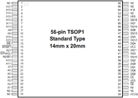
| Pin | Usage | Remarks |
|---|---|---|
| 1 | A23 | No Connection for S29GL128N |
| 2 | A22 | |
| 3 | A15 | |
| 4 | A14 | |
| 5 | A13 | |
| 6 | A12 | |
| 7 | A11 | |
| 8 | A10 | |
| 9 | A9 | |
| 10 | A8 | |
| 11 | A19 | |
| 12 | A20 | |
| 13 | WE# | Write Enable |
| 14 | RESET# | Reset |
| 15 | A21 | |
| 16 | WP#/ACC | Write Protect / Accelerated Program Operation |
| 17 | RD/BY# | Ready/Busy Output |
| 18 | A18 | |
| 19 | A17 | |
| 20 | A7 | |
| 21 | A6 | |
| 22 | A5 | |
| 23 | A4 | |
| 24 | A3 | |
| 25 | A2 | |
| 26 | A1 | |
| 27 | NC | No Connection |
| 28 | NC | No Connection |
| Pin | Usage | Remarks |
|---|---|---|
| 29 | Vio | Vio - Output Buffer Power |
| 30 | NC | No Connection |
| 31 | A0 | |
| 32 | CE# | Chip Enable |
| 33 | VSS | Ground |
| 34 | OE# | Output Enable |
| 35 | DQ0 | |
| 36 | DQ8 | |
| 37 | DQ1 | |
| 38 | DQ9 | |
| 39 | DQ2 | |
| 40 | DQ10 | |
| 41 | DQ3 | |
| 42 | DQ11 | |
| 43 | Vcc | Vcc (min 2.7V-max 3.6V / typ 3.0V) |
| 44 | DQ4 | |
| 45 | DQ12 | |
| 46 | DQ5 | |
| 47 | DQ13 | |
| 48 | DQ6 | *OTP? |
| 49 | DQ14 | |
| 50 | DQ7 | *OTP? |
| 51 | DQ15/A-1 | |
| 52 | VSS | Ground |
| 53 | #BYTE | BYTE# Selects 8-bit or 16-bit mode (NC on Samsung NOR) |
| 54 | A16 | |
| 55 | NC | No Connection |
| 56 | A24 | No Connection for S29GL128N and S29GL256N |
Samsung K8Q2815UQB-PI4B
productcode meaning:
K - Memory
8 - NOR Flash
Q - Small Classification : Page Mode DDP
28 - Density : 128M, 8M / 16Bank / 8^8
15 - Dual Bank Boot Block (Bank1, Bank2) : 16M, 2M / 14M
U - Vcc : 3.0V / 3.3V (2.7V~3.6V)
Q - Device Type: Yop and Bottom Boot Block
B - Generation : 3rd Generation
-
P - Package : TSOP1 (Lead Free)
I - Temp : Industrial
4B - Speed : 60ns/25ns (Page)
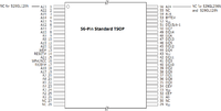
| Pin | Usage | Remarks |
|---|---|---|
| 1 | NC | No Connection |
| 2 | A22 | |
| 3 | A15 | |
| 4 | A14 | |
| 5 | A13 | |
| 6 | A12 | |
| 7 | A11 | |
| 8 | A10 | |
| 9 | A9 | |
| 10 | A8 | |
| 11 | A19 | |
| 12 | A20 | |
| 13 | WE | Write Enable |
| 14 | RESET | Reset |
| 15 | A21 | |
| 16 | WP/ACC | Write Protect / Accelerated Program Operation |
| 17 | RD/BY | Ready/Busy Output |
| 18 | A18 | |
| 19 | A17 | |
| 20 | A7 | |
| 21 | A6 | |
| 22 | A5 | |
| 23 | A4 | |
| 24 | A3 | |
| 25 | A2 | |
| 26 | A1 | |
| 27 | NC | No Connection |
| 28 | NC | No Connection |
| Pin | Usage | Remarks |
|---|---|---|
| 29 | VCCQ | VccQ |
| 30 | NC | No Connection |
| 31 | A0 | |
| 32 | CE | Chip Enable |
| 33 | VSS | Ground |
| 34 | OE | Output Enable |
| 35 | DQ0 | |
| 36 | DQ8 | |
| 37 | DQ1 | |
| 38 | DQ9 | |
| 39 | DQ2 | |
| 40 | DQ10 | |
| 41 | DQ3 | |
| 42 | DQ11 | |
| 43 | Vcc | Vcc (min 2.7V-max 3.6V / typ 3.0V) |
| 44 | DQ4 | |
| 45 | DQ12 | |
| 46 | DQ5 | |
| 47 | DQ13 | |
| 48 | DQ6 | *OTP? |
| 49 | DQ14 | |
| 50 | DQ7 | *OTP? |
| 51 | DQ15 | |
| 52 | VSS | Ground |
| 53 | NC | No Connection |
| 54 | A16 | |
| 55 | NC | No Connection |
| 56 | NC | No Connection |
- OTP Block Region : 256-word Flash memory region. The data DQ6=1 for customer locked and DQ7=1 for factory locked
Other
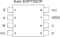
Renesas HN58X2504TIE
productcode meaning:
H -
N -
5 -
8 - Organisation : x8bit
X -
2 -
5 -
0 -
4 - Density : 4-kbit (512x8bit)
T - Package : 8pin plastic TSSOP (TTP-8DAV)
I - Temp : Industrial (-40 to +85 °C
E - Environment : Lead Free
Each PS3 has a special EEPROM chip on the motherboard using a SPI Serial Interface Renasas chip.
| Type | Size | Speed | Voltage | Packaging | Manufacturer | Serial Number | Description |
|---|---|---|---|---|---|---|---|
| EEPROM | 4-kbit (512x8bit) | 3MHz | 1.8V to 5.5V | 8-pin TSSOP | Renesas | HN58X2504TIE | PS3 EEPROM chip |
| Pin | Usage | Remarks |
|---|---|---|
| 1 | S | Chip Select |
| 2 | Q | Serial data output |
| 3 | W | Write Protect |
| 4 | VSS | Ground |
| 5 | D | Serial data input |
| 6 | C | Serial Clock |
| 7 | HOLD | Hold |
| 8 | VCC | Vcc (min 1.8V-max 5.5V) |
