File:Teensy++ 2.0 schematic.jpg
Teensy++_2.0_schematic.jpg (458 × 528 pixels, file size: 67 KB, MIME type: image/jpeg)
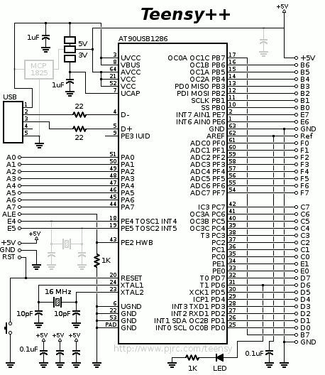
Teensy++ 2.0 schematic
A 3.3 volt MCP1825 voltage regulator (shown in gray, full part number MCP1825S-3302E/DB) may be soldered to the bottom side. Three pads allow a solder bridge to configure for 5 volt or 3.3 volt power. The 5 volt pads are linked when the board is shipped.
Four extra parts may be soldered to the bottom side of the Teensy++. These are shown in gray. A 32768 Hz crystal may be connected to E4 & E5 for the timer2 oscillator. An extra power supply decoupling capacitor may also be added, located close to the AVcc pin.
The ALE pad should only be used as an output signal. If this pin is driven high while the reset button is pressed and released, the board will not run the Halfkay bootloader.
File history
Click on a date/time to view the file as it appeared at that time.
| Date/Time | Thumbnail | Dimensions | User | Comment | |
|---|---|---|---|---|---|
| current | 18:59, 5 August 2015 | | 458 × 528 (67 KB) | Sandungas (talk | contribs) | Category:HardwareTeensy++ 2.0 schematic |
You cannot overwrite this file.
File usage
The following page uses this file: