Template:RSX pad layout 34x34: Difference between revisions
Jump to navigation
Jump to search
No edit summary |
No edit summary |
||
| Line 3: | Line 3: | ||
---- | ---- | ||
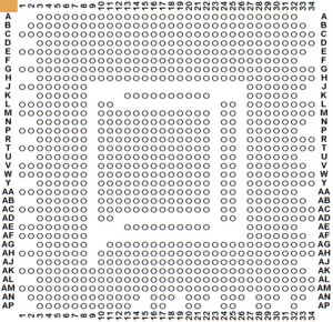
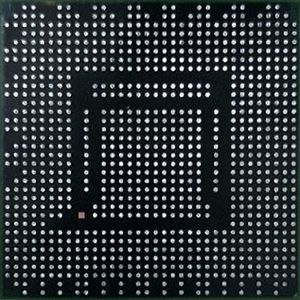
</includeonly><div style="float:right">[[File:D5305-bottom-pad-layout-transparent.png|300px|thumbnail|right|[[RSX]] D5305 Series pad layout<br />PCB view facing BGA<br />A1 marker:northwest/topleft]]<br>[[File:RSX pad layout 34x34. RSX view Photo.jpg|300px|thumbnail|right|[[RSX]] pad layout 34x34. '''RSX view''' (Photo)]]</div> | </includeonly><div style="float:right">[[File:D5305-bottom-pad-layout-transparent.png|300px|thumbnail|right|[[RSX]] D5305 Series pad layout<br />PCB view facing BGA<br />A1 marker:northwest/topleft]]<br>[[File:RSX pad layout 34x34. RSX view Photo.jpg|300px|thumbnail|right|[[RSX]] pad layout 34x34. '''RSX view''' (Photo)]]</div> | ||
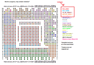
[[File:28nm_Map_attempt.png|300px|thumbnail|right|[[RSX]] D5305 pinout attempt by tracing copper tracks]]<br> | |||
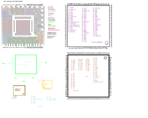
[[File:28nm_%2B_other_components_map.png|300px|thumbnail|right|[[RSX]] D5305 pinout and related components based on a NPX-001 board]]<br> | |||
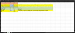
[[File:28nm-voltages.JPG|300px|thumbnail|right|[[RSX]] D5305 vs CXD2971GB voltages]]<br> | |||
<div style="overflow:auto; <includeonly>height:750px;</includeonly>"> | <div style="overflow:auto; <includeonly>height:750px;</includeonly>"> | ||
