Media: Difference between revisions
Jump to navigation
Jump to search
Cfwprophet (talk | contribs) (→Pinout) |
m (Added archive link) |
||
| (7 intermediate revisions by one other user not shown) | |||
| Line 18: | Line 18: | ||
==== Pinout ==== | ==== Pinout ==== | ||
Pinout by [[Game Card|motoharu]] | |||
{| class="wikitable sortable" style="text-align: center;border:3px dotted #123AAA;" | {| class="wikitable sortable" style="text-align: center;border:3px dotted #123AAA;" | ||
|- | |- | ||
! colspan="3" | [ | ! colspan="3" | [https://github.com/motoharu-gosuto/psvcd/raw/master/pics/pic8.png Pinout] | ||
|- | |- | ||
!! style="background-color:#ffffff; color:#123AAA;" | Pin | !! style="background-color:#ffffff; color:#123AAA;" | Pin | ||
| Line 27: | Line 28: | ||
!! style="background-color:#ffffff; color:#123AAA;" | Description | !! style="background-color:#ffffff; color:#123AAA;" | Description | ||
|- | |- | ||
| 1 || | | 1 || VCC || Voltage | ||
|- | |- | ||
| 2 || | | 2 || GND || Ground | ||
|- | |- | ||
| 3 || | | 3 || CLK || Clock | ||
|- | |- | ||
| 4 || | | 4 || D3 || Data 3 | ||
|- | |- | ||
| 5 || | | 5 || D2 || Data 2 | ||
|- | |- | ||
| 6 || | | 6 || D1 || Data 1 | ||
|- | |- | ||
| 7 || | | 7 || D0 || Data 0 | ||
|- | |- | ||
| 8 || | | 8 || INS || Detection Pin | ||
|- | |- | ||
| 9 || | | 9 || CMD || Command | ||
|- | |- | ||
| 10 || | | 10 || GND || Ground | ||
|- | |- | ||
|} | |} | ||
<gallery> | <gallery> | ||
| Line 77: | Line 79: | ||
==== Pinout ==== | ==== Pinout ==== | ||
Don't try to take it apart [http://imgur.com/a/yvFYG like this] ([https://web.archive.org/web/20230505050035/https://imgur.com/a/yvFYG archive]) | |||
see also [[Memory Card#Pinout|Memory Card]] | |||
{| class="wikitable" | {| class="wikitable" | ||
|- | |- | ||
| Line 88: | Line 93: | ||
| 3 || VCC || Voltage | | 3 || VCC || Voltage | ||
|- | |- | ||
| 4 || | | 4 || D3 || Data 3 | ||
|- | |- | ||
| 5 || | | 5 || D2 || Data 2 | ||
|- | |- | ||
| 6 || D1 || Data 1 | | 6 || D1 || Data 1 | ||
| Line 102: | Line 107: | ||
|} | |} | ||
see also [[Memory Card#Pinout|Memory Card]] | |||
==== Pinout standard SD (for comparison) ==== | ==== Pinout standard SD (for comparison) ==== | ||
Latest revision as of 06:03, 5 May 2023
PS Vita Cards[edit | edit source]
Two types of cards: Gamecards (on which games are sold) and Memorycards (to hold your savedata for games that don't use the storage on the Gamecards)
PS Vita Gamecards[edit | edit source]
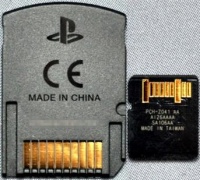
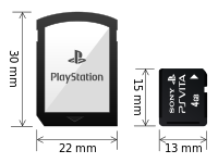
10 pin SD sized card (physical incompatible). ±1.4mm pitch.
Savegames stored on the Gamecards cannot be copied/exported.
Currently produced as 2GB and 4GB cards.
How to disassemble vita game cartridges (and reassemble it)
Pinout[edit | edit source]
Pinout by motoharu
| Pinout | ||
|---|---|---|
| Pin | Signal | Description |
| 1 | VCC | Voltage |
| 2 | GND | Ground |
| 3 | CLK | Clock |
| 4 | D3 | Data 3 |
| 5 | D2 | Data 2 |
| 6 | D1 | Data 1 |
| 7 | D0 | Data 0 |
| 8 | INS | Detection Pin |
| 9 | CMD | Command |
| 10 | GND | Ground |
PS Vita Memorycards[edit | edit source]
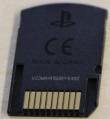
PS Vita memory cards come in five variants:
- 4 GB (€ 12 to € 30 -> €3 to 7,5 per GB)
- 8 GB (€ 26 to € 46 -> €3,25 to € 5,75 per GB)
- 16 GB (€ 35 to € 55 -> €2,1875 to € 3,4375 per GB)
- 32 GB (€ 65,- -> € 2,03125 per GB)
- 64 GB (9580 yen, ~$94 -> $1,46875 per GB)
note: current sales price as listed in Pricewatch
Pinout[edit | edit source]
Don't try to take it apart like this (archive)
see also Memory Card
| Pin | Signal | Description |
|---|---|---|
| 1 | INS | Detection Pin |
| 2 | SCLK | Serial Clock |
| 3 | VCC | Voltage |
| 4 | D3 | Data 3 |
| 5 | D2 | Data 2 |
| 6 | D1 | Data 1 |
| 7 | D0 | Data 0 |
| 8 | BS | Bus State |
| 9 | VSS | Ground |
see also Memory Card
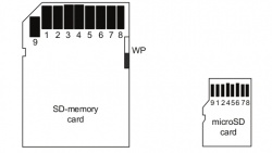
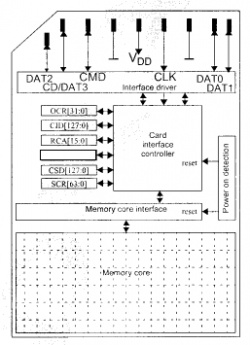
Pinout standard SD (for comparison)[edit | edit source]
| in SD Card Mode | ||||
|---|---|---|---|---|
| Pin № | Name | I/O | Logic | Description |
| 1 | DAT3 | I/O | PP | Data 3 |
| 2 | CMD | I/O | PP,OD | Command, Response |
| 3 | VSS1 | S | S | Ground |
| 4 | VDD | S | S | Power |
| 5 | CLK | I | PP | Clock |
| 6 | VSS2 | S | S | Ground |
| 7 | DAT0 | I/O | PP | Data 0 |
| 8 | DAT1 nIRQ |
I/O O |
PP OD |
Data 1. SDIO Cards share with Interrupt Period |
| 9 | DAT2 | I/O | PP | Data 2 |
Notes:
- Direction is relative to card. I = Input, O = Output.
- PP = Push-Pull logic, OD = Open-Drain logic.
- S = Power Supply, NC = Not Connected (or logical high).
- The extended DAT lines (DAT1-DAT3) are input on power up. They start to operate as DAT lines after the SET_BUS_WIDTH command.
It is the responsibility of the host designer to connect external pullup resistors to all data lines even if only DAT0 is to be used.
Otherwise, non-expected high current consumption may occur due to the floating inputs of DAT1 & DAT2 (in case they are not used). - After power up, DAT3 is input with 50Kohm(+/-20Kohm) pull-up (can be used for card detection or SPI mode selection.
The pull-up may be disconnected by the user, during regular data transfer, with SET_CLR_CARD_DETECT (ACMD42) command.
| in SPI Mode | |||
|---|---|---|---|
| Pin № | Name | Type | Description |
| 1 | CS | I | Host to card Chip Select signal (Active low) |
| 2 | DataIn | I | Host to card data signal |
| 3 | VSS1 | S | Ground |
| 4 | VDD | S | Power |
| 5 | CLK | I | Host to card clock signal |
| 6 | VSS2 | S | Ground |
| 7 | DATOut | O/PP | Card to host data signal |
| 8 | RSV | I | Reserved |
| 9 | RSV | I | Reserved |
