Baryon: Difference between revisions
Jump to navigation
Jump to search
m (Text replacement - "<imgur(?:\s+\w+=(?:\w+|"[^"]+"))*\s*>([^<]+?\.(jpg|jpeg|png|gif))\s*<\/imgur>" to "File:$1") |
|||
| (39 intermediate revisions by 6 users not shown) | |||
| Line 6: | Line 6: | ||
! Version | ! Version | ||
! Notes | ! Notes | ||
|- | |||
| 0x00010600 | |||
| From MVG's Japan Import PSP | |||
|- | |- | ||
| 0x00020601 | | 0x00020601 | ||
| Line 11: | Line 14: | ||
|- | |- | ||
| 0x00030600 | | 0x00030600 | ||
| | | Found on TA-079 | ||
|- | |||
| 0x00030601 | |||
| Found on TMU-002 | |||
|- | |- | ||
| 0x00040600 | | 0x00040600 | ||
| Line 51: | Line 57: | ||
| 0x00403000 | | 0x00403000 | ||
| | | | ||
|} | |||
<pre> | |||
First: | |||
0x00010600 D780032AY BARxx | |||
0x00020600 D780032AY BARxx | |||
0x00020601 D780032AY BARxx | |||
0x00030600 D780032AY BARxx | |||
0x00030601 D780032AY BARxx | |||
0x00040600 D780032AY BARxx | |||
Legolas 1: | |||
0x00114000 D78F0531 B30x | |||
Legolas 2: | |||
0x00121000 D78F0531 B30x | |||
Frodo: | |||
0x0022B200 D78F0544 B40x | |||
0x00234000 D78F0544 B40x | |||
0x00243000 D78F0544 B40x | |||
Samwise: | |||
0x00263100 D78F0534 3Axx | |||
0x00285000 D78F0534 3Axx | |||
Samwise VA2: | |||
0x002C4000 D78F0534 3Bxx | |||
0x002E4000 D78F0534 3Bxx | |||
Strider: | |||
0x00304000 D78F0544 40xx | |||
</pre> | |||
= Chip 4 Digit Comparison with Motherboard = | |||
{| class="wikitable" style="text-align: center" | |||
! Motherboard !! Version | |||
|- | |||
| TA-085 || B401 | |||
|- | |||
| TA-088 || B403 | |||
|- | |||
| TA-090 || 3A01 | |||
|- | |||
| TA-091 || 4053 | |||
|- | |||
| TA-092 || 3A47 | |||
|- | |||
| TA-093 || 3B58 | |||
|- | |||
| TA-095 || 3B41 | |||
|- | |||
| TA-096 || 3B57 | |||
|- | |||
|} | |} | ||
= Hardware = | = Hardware = | ||
== TA-096 Buttons == | |||
<pre> | |||
E4 - RTrigger | |||
E8 - Cross | |||
E5 - Square | |||
D7 - Circle | |||
E7 - Triangle | |||
F4 - LTrigger | |||
D8 - LeftDpad | |||
D6 - RightDpad | |||
D5 - UpDpad | |||
D4 - DownDpad | |||
A7 - Vol- | |||
B7 - Vol+ | |||
E2 - Home | |||
</pre> | |||
== About 84 pin BGA Legenda == | |||
<pre> | |||
Black-VSS | |||
Red-VDD | |||
Blue-OCD0a | |||
Brown-OCD0b | |||
Orange-FLMD0 | |||
Pink-REGC | |||
Green-Reset | |||
Yellow-TX | |||
Cyan-RX | |||
</pre> | |||
== Hardware versions == | == Hardware versions == | ||
| Line 59: | Line 153: | ||
* Note: You can usually deduce the serial number of the system controller chip on the motherboard when knowing Baryon version. For example, 0x00030600 has the BAR14 labelled chip, while 0x00040600 has the BAR15 labelled chip. | * Note: You can usually deduce the serial number of the system controller chip on the motherboard when knowing Baryon version. For example, 0x00030600 has the BAR14 labelled chip, while 0x00040600 has the BAR15 labelled chip. | ||
== | == Talking to Baryon == | ||
<pre> | <pre> | ||
TA-086: | |||
- Power from programmer (3.3V) | |||
- X1 OSC 4Mhz | |||
- Cut FLMD0 grounding | |||
========== (Connect) ========== | |||
------ Start(Signature Read) ------ | |||
Device name: UPD78F0531 | |||
Device data: 10 7F 04 7C | |||
Device end addr: 00003FFF | |||
Security Flag: 00FF (Vulnerable) | |||
Boot Block Number: 003 | |||
Firmware Version: 2.00 | |||
Signature Read PASS | |||
------ End(Signature Read) ------ | |||
========== (Disconnect) ========== | |||
TA-085: | |||
- Power from programmer (3.3V) | |||
- X1 OSC 4Mhz | |||
========== (Connect) ========== | |||
------ Start(Signature Read) ------ | |||
Device name: UPD78F0544 | |||
Device data: 10 7F 04 7C | |||
Device end addr: 0000BFFF | |||
Security Flag: 00F9 | |||
Boot Block Number: 003 | |||
Firmware Version: 2.00 | |||
Signature Read PASS | |||
------ End(Signature Read) ------ | |||
========== (Disconnect) ========== | |||
TA-093: | |||
- Power from programmer (3.3V) | |||
- EXCLK (OCD0B) 4Mhz from Programmer | |||
========== (Connect) ========== | |||
------ Start(Signature Read) ------ | |||
Device name: UPD78F0534 | |||
Device data: 10 7F 04 7C | |||
Device end addr: 0000BFFF | |||
Security Flag: 00E8 | |||
Boot Block Number: 003 | |||
Firmware Version: 2.00 | |||
Signature Read PASS | |||
------ End(Signature Read) ------ | |||
========== (Disconnect) ========== | |||
TA-091: | |||
- Power from programmer (3.3V) | |||
- EXCLK (OCD0B) 4Mhz from Programmer | |||
- Remove RxD/TxD resistors | |||
========== (Connect) ========== | |||
------ Start(Signature Read) ------ | |||
Device name: UPD78F0544 | |||
Device data: 10 7F 04 7C | |||
Device end addr: 0000BFFF | |||
Security Flag: 00F9 | |||
Boot Block Number: 003 | |||
Firmware Version: 2.00 | |||
Signature Read PASS | |||
------ End(Signature Read) ------ | |||
========== (Disconnect) ========== | |||
TA-090: | |||
========== (Connect) ========== | |||
------ Start(Signature Read) ------ | |||
Device name: UPD78F0534 | |||
Device data: 10 7F 04 7C | |||
Device end addr: 0000BFFF | |||
Security Flag: 00F9 | |||
Boot Block Number: 003 | |||
Firmware Version: 2.00 | |||
Signature Read PASS | |||
------ End(Signature Read) ------ | |||
========== (Disconnect) ========== | |||
</pre> | |||
== Hardware Signature (3AXX) == | |||
<pre> | |||
10 7F 04 7C 7F 7F 02 C4 37 38 46 B0 B5 B3 34 20 20 79 03 | |||
</pre> | </pre> | ||
== Hardware Revision ( | == Meaning == | ||
<pre> | |||
10 Vendor (Renessas) | |||
7F Extension code (fixed in 78K0/Kx2) | |||
04 Function information (fixed in 78K0/Kx2) | |||
7C Device Extension code (fixed in 78K0/Kx2) | |||
7F 7F 02 Internal flash memory last address (extracted from the lower bytes) (0xBFFF) (48KB) (Note 2) | |||
C4 37 38 46 B0 B5 B3 34 20 20 Device name (D78F0534 ) | |||
79 Security flag information (odd parity bit so 0xF9) (Note 3) | |||
03 Boot block number (fixed) | |||
</pre> | |||
=== Notes === | |||
<pre> | |||
Note 2. | |||
The parity calculation for the END field is performed as follows (when the last address is 005FFFH) | |||
<1> The END field is divided in 7-bit units from the lower digit (the higher 3 bits are discarded). | |||
0 0 5 F F F 00000000 01011111 11111111 ↓ 000 0000001 0111111 1111111 | |||
<2> The odd parity bit is appended to the highest bit. | |||
p0000001 p01111111 p1111111 (p = odd parity bit) = 0000001 10111111 01111111 = 01 BF 7F | |||
<3> The order of the higher, middle, and lower bytes is reversed, as follows. 7F BF 01 | |||
CHAPTER 5 DESCRIPTION OF COMMAND PROCESSING | |||
Application Note U17739EJ2V0AN 50 | |||
The following shows the procedure to translate the values in the END field that has been sent from the microcontroller to the actual address. | |||
<1> The order of the higher, middle, and lower bytes is reversed, as follows. | |||
7F BF 01 ↓ 01 BF 7F | |||
<2> Checks that the number of “1” is odd in each byte (this can be performed at another timing). | |||
<3> The parity bit is removed and a 3-bit 0 is added to the highest bit. | |||
01 BF 7F ↓ 00000001 10111111 01111111 ↓ 0000001 0111111 1111111 ↓ 000 0000001 0111111 1111111 | |||
<4> The values are translated into groups in 8-bit units. | |||
00000000101111111111111 ↓ 00000000 01011111 11111111 ↓ = 0 0 5 F F F | |||
If “7F BF 01” is given to the END field, the actual last address is consequently 005FFFH. | |||
</pre> | |||
<pre> | |||
Note 3. When security flag information is set using the Security Set command, the highest bit is fixed to “1”. If the security flag information is read using the Silicon Signature command, however, the highest bit is the odd parity. | |||
</pre> | |||
== Hardware Revision (3AXX) == | |||
<pre> | <pre> | ||
| Line 74: | Line 305: | ||
* 48 KB FLASH | * 48 KB FLASH | ||
* 1KB RAM | * 1KB RAM | ||
* 4 MHz | |||
* Multiplier x1 | |||
* UART-X1-OSC | |||
* If 64 Pin, REGC Connected to VDD (for some odd reason) | |||
= Pictures = | = Pictures = | ||
[[File:hzFRdIn.jpg]] | |||
[[File:32tdUCq.png]] | |||
[[File:YphArDh.png]] | |||
[[File:Bu2tbIC.png]] | |||
[[File:SogMH5i.png]] | |||
[[File:13bzl4B.png]] | |||
= Notes on TA-086 psp syscon firmware = | |||
* Sbox at 0x3E00 (size 0x100) | |||
* Keys at 0x3F00 (size 0xC0) | |||
* Syscon Version at 0x3FC0 size 4 endian swapped (Baryon:0×00121000) | |||
* Syscon Build Date at 0x3FC4 size 0x1C ($Date: 2005/12/20 05:58:05 $) | |||
<pre> | |||
External (0x8522-0x854B): | |||
00 0x80F3 Reset | |||
20 0x93FF Chip Erase | |||
22 0x942F Block Erase | |||
13 0x9379 Verify | |||
32 0x9609 Block Blank Check | |||
40 0x969F Programming | |||
90 0x9994 Oscillating Frequency Set | |||
9E 0x99ED ?? | |||
C0 0x9B08 Silicon Signature | |||
C5 0x9B71 Version Get | |||
70 0x9A5B Status | |||
B0 0x9A79 Checksum | |||
A0 0x9C04 Security Set | |||
A4 0x9B97 ?? | |||
Internal (0x9FC9 - 0x9FE6): | |||
17 0x8218 EEPROMWrite | |||
0F 0x84B3 ?? | |||
0E 0x84A8 CheckFLMD | |||
0A 0x8475 FlashSetInfo | |||
09 0x8399 FlashGetInfo | |||
08 0x835D FlashBlockBlankCheck | |||
06 0x8321 FlashBlockVerify | |||
04 0x8252 FlashWordWrite | |||
03 0x81DD FlashBlockErase | |||
00 0x81BD FlashEnv | |||
</pre> | |||
Latest revision as of 05:55, 4 May 2023
Baryon is the codename for the PSP Syscon (System Controller) chip. Communication with this chip is done through SPI.
Versions[edit | edit source]
| Version | Notes |
|---|---|
| 0x00010600 | From MVG's Japan Import PSP |
| 0x00020601 | First known version. Found on TMU-001 motherboard. |
| 0x00030600 | Found on TA-079 |
| 0x00030601 | Found on TMU-002 |
| 0x00040600 | |
| 0x00114000 | |
| 0x00121000 | |
| 0x0022B200 | |
| 0x00234000 | Removed ability to write to battery EEPROM. |
| 0x00243000 | |
| 0x00263100 | |
| 0x00285000 | |
| ?0x002A0000? | From hypothetical TA-094 motherboard. |
| 0x002C4000 | |
| 0x002E4000 | |
| 0x00304000 | |
| 0x00403000 |
First:
0x00010600    D780032AY  BARxx
0x00020600    D780032AY  BARxx
0x00020601    D780032AY  BARxx
0x00030600    D780032AY  BARxx
0x00030601    D780032AY  BARxx
0x00040600    D780032AY  BARxx

Legolas 1:
0x00114000    D78F0531  B30x

Legolas 2:
0x00121000    D78F0531  B30x

Frodo:
0x0022B200    D78F0544  B40x
0x00234000    D78F0544  B40x
0x00243000    D78F0544  B40x

Samwise:
0x00263100    D78F0534  3Axx
0x00285000    D78F0534  3Axx

Samwise VA2:
0x002C4000    D78F0534  3Bxx
0x002E4000    D78F0534  3Bxx

Strider:
0x00304000    D78F0544  40xx
Chip 4 Digit Comparison with Motherboard[edit | edit source]
| Motherboard | Version |
|---|---|
| TA-085 | B401 |
| TA-088 | B403 |
| TA-090 | 3A01 |
| TA-091 | 4053 |
| TA-092 | 3A47 |
| TA-093 | 3B58 |
| TA-095 | 3B41 |
| TA-096 | 3B57 |
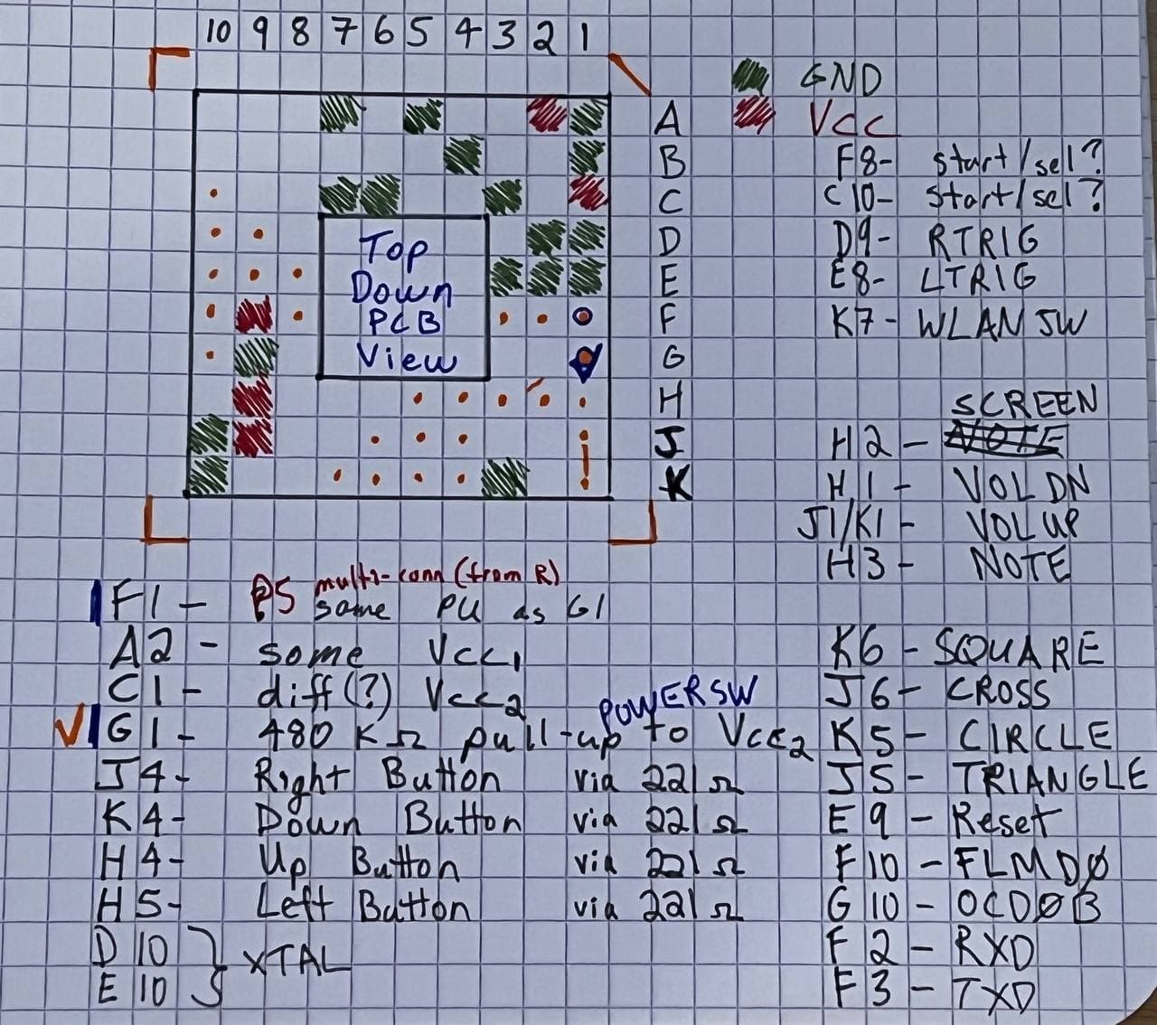
Hardware[edit | edit source]
TA-096 Buttons[edit | edit source]
E4 - RTrigger
E8 - Cross
E5 - Square
D7 - Circle
E7 - Triangle


F4 - LTrigger
D8 - LeftDpad
D6 - RightDpad
D5 - UpDpad
D4 - DownDpad

A7 - Vol-
B7 - Vol+
E2 - Home
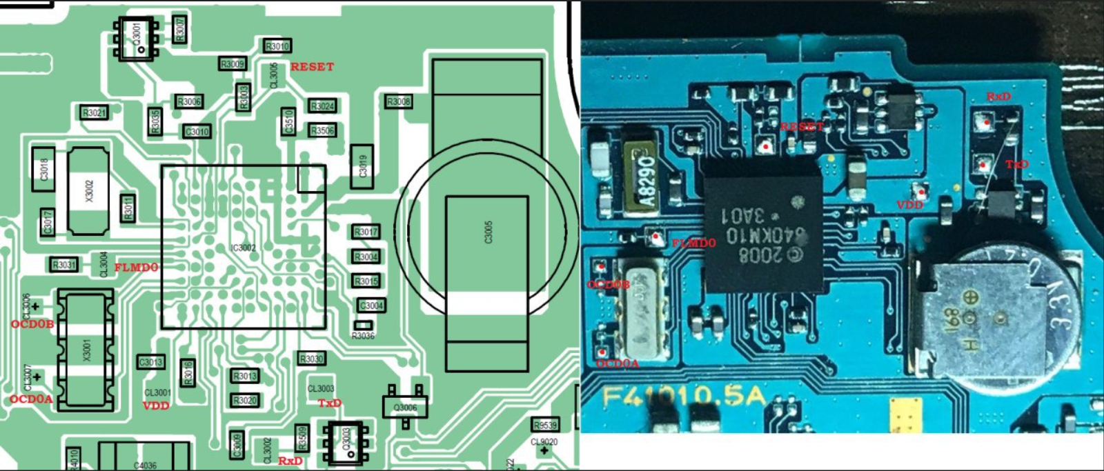
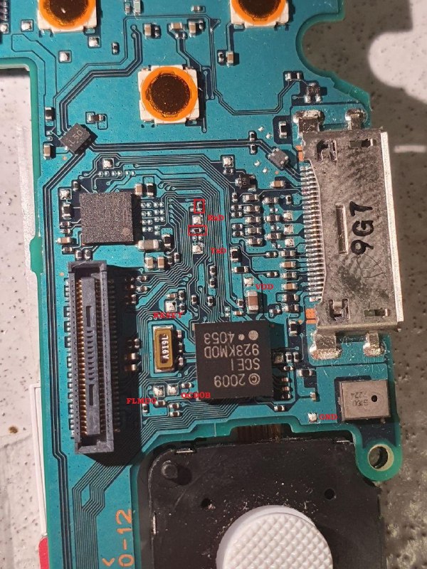
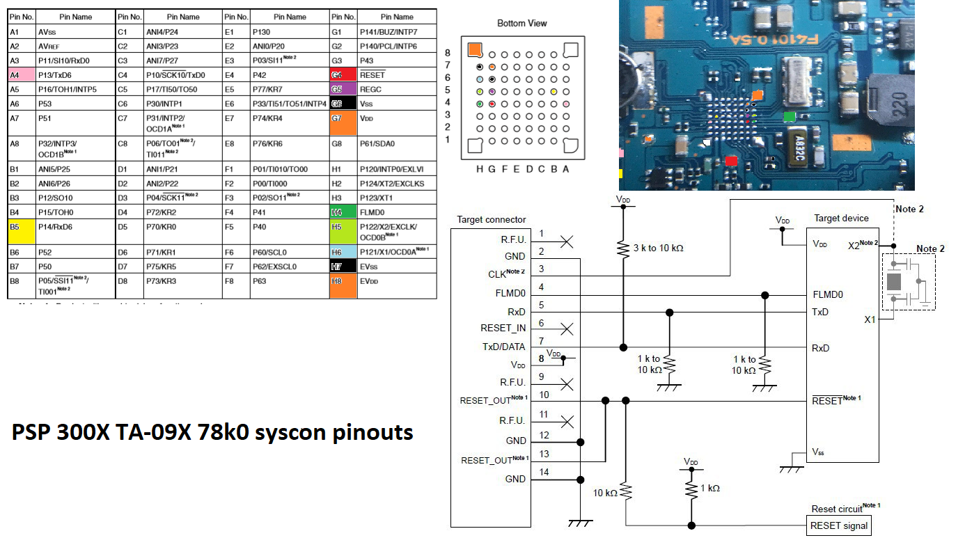
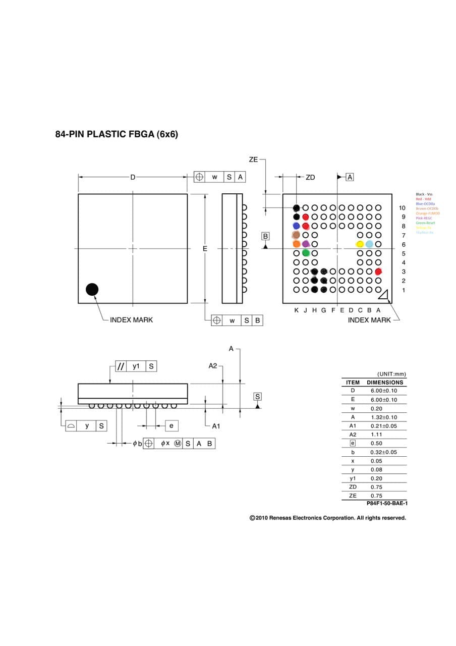
About 84 pin BGA Legenda[edit | edit source]
Black-VSS
Red-VDD
Blue-OCD0a
Brown-OCD0b
Orange-FLMD0
Pink-REGC
Green-Reset
Yellow-TX
Cyan-RX
Hardware versions[edit | edit source]
- Note: You can usually deduce the serial number of the system controller chip on the motherboard when knowing Baryon version. For example, 0x00030600 has the BAR14 labelled chip, while 0x00040600 has the BAR15 labelled chip.
Talking to Baryon[edit | edit source]
TA-086:
- Power from programmer (3.3V)
- X1 OSC 4Mhz
- Cut FLMD0 grounding
========== (Connect) ==========
------ Start(Signature Read) ------
Device name: UPD78F0531
Device data:  10 7F 04 7C
Device end addr: 00003FFF
Security Flag: 00FF (Vulnerable)
Boot Block Number: 003
Firmware Version: 2.00
Signature Read PASS
------ End(Signature Read) ------
========== (Disconnect) ==========


TA-085:
- Power from programmer (3.3V)
- X1 OSC 4Mhz
========== (Connect) ==========
------ Start(Signature Read) ------
Device name: UPD78F0544
Device data:  10 7F 04 7C
Device end addr: 0000BFFF
Security Flag: 00F9
Boot Block Number: 003
Firmware Version: 2.00
Signature Read PASS
------ End(Signature Read) ------
========== (Disconnect) ==========


TA-093:
- Power from programmer (3.3V)
- EXCLK (OCD0B) 4Mhz from Programmer
========== (Connect) ==========
------ Start(Signature Read) ------
Device name: UPD78F0534
Device data:  10 7F 04 7C
Device end addr: 0000BFFF
Security Flag: 00E8
Boot Block Number: 003
Firmware Version: 2.00
Signature Read PASS
------ End(Signature Read) ------
========== (Disconnect) ==========

TA-091:
- Power from programmer (3.3V)
- EXCLK (OCD0B) 4Mhz from Programmer
- Remove RxD/TxD resistors
========== (Connect) ==========
------ Start(Signature Read) ------
Device name: UPD78F0544
Device data:  10 7F 04 7C
Device end addr: 0000BFFF
Security Flag: 00F9
Boot Block Number: 003
Firmware Version: 2.00
Signature Read PASS
------ End(Signature Read) ------
========== (Disconnect) ==========


TA-090:
========== (Connect) ==========
------ Start(Signature Read) ------
Device name: UPD78F0534
Device data:  10 7F 04 7C
Device end addr: 0000BFFF
Security Flag: 00F9
Boot Block Number: 003
Firmware Version: 2.00
Signature Read PASS
------ End(Signature Read) ------
========== (Disconnect) ==========
Hardware Signature (3AXX)[edit | edit source]
10 7F 04 7C 7F 7F 02 C4 37 38 46 B0 B5 B3 34 20 20 79 03
Meaning[edit | edit source]
10 Vendor (Renessas)
7F Extension code (fixed in 78K0/Kx2)
04 Function information (fixed in 78K0/Kx2)
7C Device Extension code (fixed in 78K0/Kx2)
7F 7F 02 Internal flash memory last address (extracted from the lower bytes)  (0xBFFF) (48KB) (Note 2)
C4 37 38 46 B0 B5 B3 34 20 20 Device name (D78F0534  )
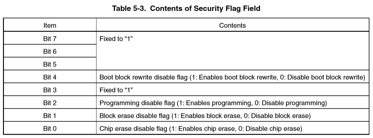
79 Security flag information (odd parity bit so 0xF9) (Note 3)
03 Boot block number (fixed)
Notes[edit | edit source]
Note 2.
The parity calculation for the END field is performed as follows (when the last address is 005FFFH)

<1> The END field is divided in 7-bit units from the lower digit (the higher 3 bits are discarded).

    0  0     5 F     F F 00000000 01011111 11111111  ↓  000  0000001  0111111  1111111

<2> The odd parity bit is appended to the highest bit.

    p0000001  p01111111  p1111111 (p = odd parity bit)  = 0000001  10111111  01111111  = 01 BF 7F

<3> The order of the higher, middle, and lower bytes is reversed, as follows.    7F BF 01

CHAPTER  5   DESCRIPTION  OF  COMMAND  PROCESSING
Application Note  U17739EJ2V0AN 50
  The following shows the procedure to translate the values in the END field that has been sent from the microcontroller to the actual address.

<1> The order of the higher, middle, and lower bytes is reversed, as follows.

 7F BF 01       ↓  01 BF 7F

<2> Checks that the number of “1” is odd in each byte (this can be performed at another timing).

<3> The parity bit is removed and a 3-bit 0 is added to the highest bit.

 01 BF 7F       ↓  00000001  10111111  01111111       ↓  0000001    0111111  1111111       ↓  000  0000001  0111111  1111111

<4> The values are translated into groups in 8-bit units.

 00000000101111111111111       ↓  00000000  01011111  11111111       ↓  =     0     0       5     F       F     F

  If “7F BF 01” is given to the END field, the actual last address is consequently 005FFFH.
Note 3. When security flag information is set using the Security Set command, the highest bit is fixed to “1”. If the security flag information is read using the Silicon Signature command, however, the highest bit is the odd parity.
Hardware Revision (3AXX)[edit | edit source]
D78F0534
- custom BGA 78K0/KE2
- 48 KB FLASH
- 1KB RAM
- 4 MHz
- Multiplier x1
- UART-X1-OSC
- If 64 Pin, REGC Connected to VDD (for some odd reason)
Pictures[edit | edit source]
Notes on TA-086 psp syscon firmware[edit | edit source]
- Sbox at 0x3E00 (size 0x100)
- Keys at 0x3F00 (size 0xC0)
- Syscon Version at 0x3FC0 size 4 endian swapped (Baryon:0×00121000)
- Syscon Build Date at 0x3FC4 size 0x1C ($Date: 2005/12/20 05:58:05 $)
External (0x8522-0x854B):

00 0x80F3 Reset
20 0x93FF Chip Erase
22 0x942F Block Erase
13 0x9379 Verify
32 0x9609 Block Blank Check
40 0x969F Programming
90 0x9994 Oscillating Frequency Set
9E 0x99ED ??
C0 0x9B08 Silicon Signature
C5 0x9B71 Version Get
70 0x9A5B Status
B0 0x9A79 Checksum
A0 0x9C04 Security Set
A4 0x9B97 ??

Internal (0x9FC9 - 0x9FE6):

17 0x8218 EEPROMWrite
0F 0x84B3 ??
0E 0x84A8 CheckFLMD
0A 0x8475 FlashSetInfo
09 0x8399 FlashGetInfo
08 0x835D FlashBlockBlankCheck
06 0x8321 FlashBlockVerify
04 0x8252 FlashWordWrite
03 0x81DD FlashBlockErase
00 0x81BD FlashEnv
