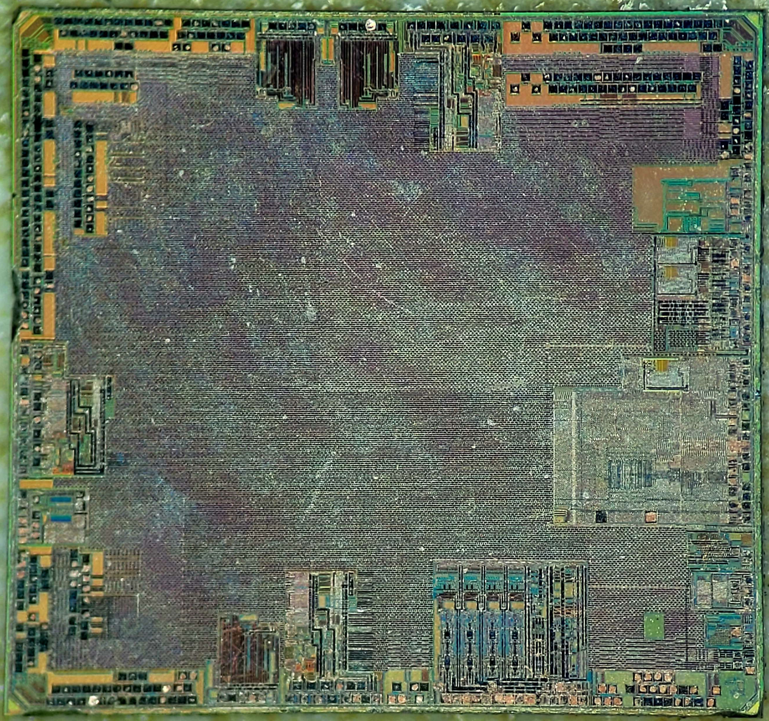
CXD90061GG: Difference between revisions
Jump to navigation
Jump to search
(Initial start to the southbridge pin out table.) |
m (Updated some southbridge pin outs.) |
||
| Line 25: | Line 25: | ||
|NC_A1 | |NC_A1 | ||
|N/C | |N/C | ||
| | |[[File:Pin-nc.png|frameless]] | ||
|NC | |NC | ||
|- | |- | ||
| Line 31: | Line 31: | ||
|NC_A2 | |NC_A2 | ||
|N/C | |N/C | ||
| | |[[File:Pin-nc.png|frameless]] | ||
|NC | |NC | ||
|- | |- | ||
|A3 | |||
|VSS_A3 | |||
|GND | |||
|[[File:IC-Pin-in.png|frameless]] | |||
|Ground | |||
|- | |||
|A4 | |||
|CK25M_FLC | |||
|S50G_FC_SYSCLK | |||
| | | | ||
|[[CXD90062GG|Flash Controller]] SYS CLOCK | |||
|- | |||
|A5 | |||
|VSS_A5 | |||
|GND | |||
|[[File:Pin-nc.png|frameless]] | |||
|Ground | |||
|- | |||
|A6 | |||
|TXVN_A_P0 | |||
|D100_SSB_GE_MDIN0 | |||
| | | | ||
| | |Connected to ethernet magnetics transformer | ||
|} | |} | ||
Revision as of 22:53, 10 December 2024
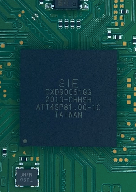
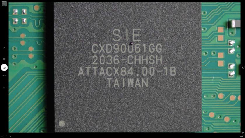
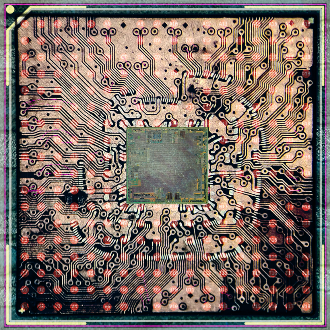
EMC/EAP Chip (with SysCon bundled?)
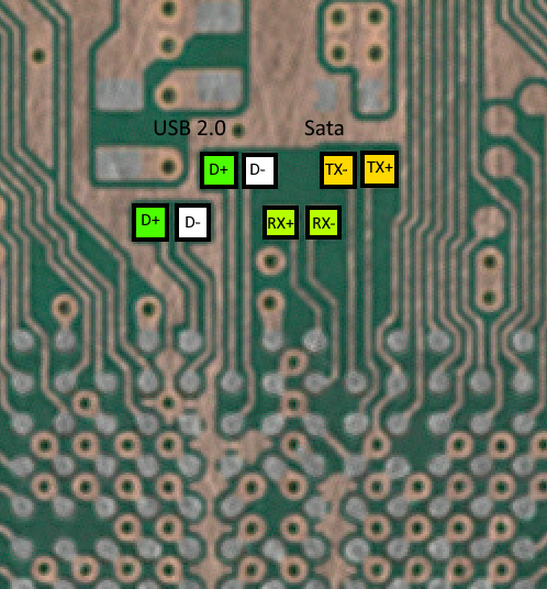
- Credit to dan2wik for the third , fourth and fifth picture
Pictures
Pinout
- TODO
| Pad | Internal | External | Type | Description |
|---|---|---|---|---|
| A1 | NC_A1 | N/C | NC | |
| A2 | NC_A2 | N/C | NC | |
| A3 | VSS_A3 | GND | Ground | |
| A4 | CK25M_FLC | S50G_FC_SYSCLK | Flash Controller SYS CLOCK | |
| A5 | VSS_A5 | GND | Ground | |
| A6 | TXVN_A_P0 | D100_SSB_GE_MDIN0 | Connected to ethernet magnetics transformer |
