Service Connectors
Service Connectors
JTAG/UART/SPI/Diagnostic I/O used in Sony repair centers if a PS3 couldn't be fixed by software.
Notes:
- EBUS and NOR Interface Testpoints are the storage related service points used with pinJIG/pogopin infactory
- PCI also has some pads for South Bridge I/O service/diagnostics.
Preproduction Generation
| Used on | Type of Connector |
|---|---|
| MPU-501 (CEB-2040) | CN6504: Headerpins CN6507: ZIF Connector |
CN6504 (SC_JTAG)

| Pin | Pogo-Pin Con. | Name | Connected to | Function | Group |
|---|---|---|---|---|---|
| 1 | NO | ? | ? | ? | |
| 2 | NO | ? | ? | ? | |
| 3 | NO | ? | ? | ? | |
| 4 | NO | ? | ? | ? | |
| 5 | NO | ? | ? | ? | |
| 6 | NO | ? | ? | ? | |
| 7 | NO | ? | ? | ? | |
| 8 | NO | ? | ? | ? | |
| 9 | NO | ? | ? | ? | |
| 10 | NO | ? | ? | ? | |
| 11 | NO | ? | ? | ? | |
| 12 | NO | ? | ? | ? | |
| 13 | NO | ? | ? | ? | |
| 14 | NO | ? | ? | ? | |
| 15 | NO | ? | ? | ? | |
| 16 | NO | ? | ? | ? | |
| 17 | NO | ? | ? | ? | |
| 18 | NO | ? | ? | ? | |
| 19 | NO | ? | ? | ? | |
| 20 | NO | ? | ? | ? |
CN6507 (STATUS)
| Pin | Pogo-Pin Con. | Name | Connected to | Function | Group |
|---|---|---|---|---|---|
| 1 | NO | ? | ? | ? | |
| 2 | NO | ? | ? | ? | |
| 3 | NO | ? | ? | ? | |
| 4 | NO | ? | ? | ? | |
| 5 | NO | ? | ? | ? | |
| 6 | NO | ? | ? | ? | |
| 7 | NO | ? | ? | ? | |
| 8 | NO | ? | ? | ? | |
| 9 | NO | ? | ? | ? |
CN6504 (SC_JTAG) (DECR)

| Pin | Pogo-Pin Con. | Name | Connected to | Function | Group |
|---|---|---|---|---|---|
| 1 | NO | GND | DC-DC Regulator | Ground line | - |
| 2 | ?? | SC_RESET/RST | Syscon | System Reset | Syscon JTAG |
| 3 | NO | +3.3V_EVER | DC-DC Regulator | +3.3V line | - |
| 4 | ?? | JRTCK | Syscon | Return Test Clock | Syscon JTAG |
| 5 | ?? | JTCK | Syscon | Test Clock | |
| 6 | ?? | JTMS | Syscon | Test Mode Select | |
| 7 | ?? | JTDO | Syscon | Test Data Out | |
| 8 | ?? | JTDI | Syscon | Test Data In | |
| 9 | ?? | JNTRST | Syscon | Test Reset | |
| 10 | NO | +3.3V_EVER | DC-DC Regulator | +3.3V line | - |
- (SC) RESET is connected to S6503 Button
Diag/Backup (DECR)
| Pin | Pogo-Pin Con. | Name | Connected to | Function | Group |
|---|---|---|---|---|---|
| - | ?? | Backup Mode? | Syscon | Backup Mode? | Syscon Modes |
| - | ?? | Diag Mode? | Syscon | Diagnose Mode? |
- Backup is Connected to S6502-1 Switch
- Diag is Connected to S6502-2 Switch
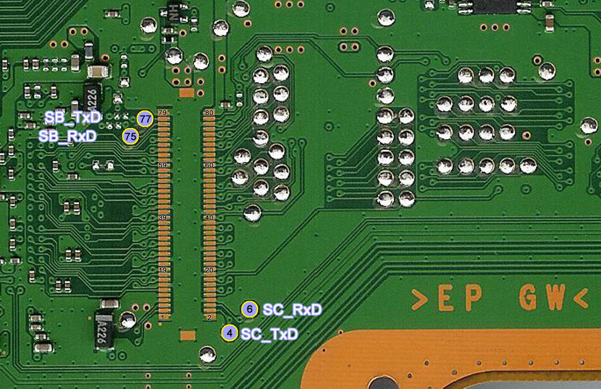
SC_UART (DECR)
| Pin | Pogo-Pin Con. | Name | Connected to | Function | Standby Voltage | Group |
|---|---|---|---|---|---|---|
| - | ?? | +3.3V_EVER? | DC-DC Regulator | +3.3V line? | 3.3 | - |
| - | ?? | Rx? | Syscon | Receive UART? | 0 | Syscon UART |
| - | ?? | Tx? | Syscon | Transfer UART? | 3.14 | |
| - | ?? | GND? | DC-DC Regulator | Ground line | 0 | - |
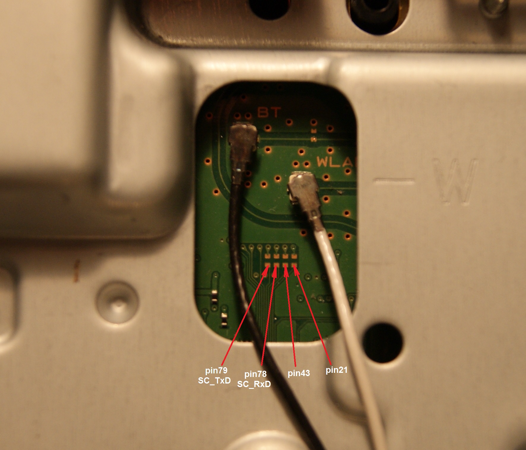
Pictures (Traces from DECR)
- JTAG/BAK/DIA/UART TX/UART RX -> https://www.psdevwiki.com/ps3/File:7eGuCpc.jpg
1st Generation
| Used on | Type of Connector |
|---|---|
| COOKIE-13 | ZIF Connector |
| COK-001 (Prototype) | Plain socket |
| COK-001 | Plain socket |
| COK-002 | Plain socket |
| COK-002W | Plain socket |
CN4009


| Pin | Pogo-Pin Con. | Name | Connected to | Function | Group |
|---|---|---|---|---|---|
| 1 | NO | +5V_EVER | DC-DC Regulator | +5V line | - |
| 2 | YES | TRST | Syscon | Test Reset (nTRST) | Syscon JTAG |
| 3 | YES | TDI | Syscon | Test Data In | |
| 4 | YES | RTCK | Syscon | Return Test Clock | |
| 5 | YES | TCK | Syscon | Test Clock | |
| 6 | YES | TDO | Syscon | Test Data Out | |
| 7 | YES | TMS | Syscon | Test Mode Select | |
| 8 | YES | SC_RESET | Syscon | System Reset (nSRST) | |
| 9 | NO | GND | DC-DC Regulator | Ground line | - |
| 10 | YES | RxD | Syscon | Serial Receive | Syscon UART |
| 11 | YES | TxD | Syscon | Serial Transmit | |
| 12 | NO | GND | DC-DC Regulator | Ground line | - |
| 13 | YES | Diag Mode | Syscon | Diagnose Mode | Syscon Modes |
| 14 | YES | Backup Mode | Syscon | Backup Mode | |
| 15 | NO | +3.3V_EVER | DC-DC Regulator | +3.3V line | - |
| 16 | YES | NC | - | - | - |
| 17 | NO | RMC | Syscon | IR Remote Control (input) | - |
| 18 | NO | SB_TxD | South Bridge | Serial Transmit | South Bridge UART |
| 19 | NO | SB_RxD | South Bridge | Serial Receive | |
| 20 | NO | SW_4_A | (W)LAN | Power Switch | LAN & WLAN |
| 21 | NO | BE_TRG_OUT | CELL BE | Trigger Out | Component Tests |
| 22 | NO | RSX_TRG_OUT | RSX | Trigger Out | |
| 23 | NO | SB_TRG_OUT | South Bridge | Trigger Out | |
| 24 | NO | BE_CHKSTP_OUT | CELL BE | Checkstop Out | |
| 25 | NO | RSX_CHKSTP_OUT | RSX | Checkstop Out | |
| 26 | NO | SB_CHKSTP_OUT | South Bridge | Checkstop Out | |
| 27 | NO | +1.2V_MC_VDDIO | DC-DC Regulator | +1.2V line | - |
| 28 | NO | +1.5V_RSX_VDDIO | DC-DC Regulator | +1.5V line | |
| 29 | NO | GND | DC-DC Regulator | Ground line | |
| 30 | NO | +5V_EVER | DC-DC Regulator | +5V line |
It looks like Kayocera 6240
CELL_BE JTAG Testpads

| Pin | Pogo-Pin Con. | Name | Connected to | Function | Group |
|---|---|---|---|---|---|
| CL1103 | YES | TDO | pin AW14 @ CELL BE | Test Data Out | CELL BE JTAG |
| CL1104 | YES | TDI | pin AW13 @ CELL BE | Test Data In | |
| CL1105 | YES | TCK | pin BA13 @ CELL BE | Test Clock | |
| CL1106 | YES | TMS | pin AW12 @ CELL BE | Test Mode Select | |
| CL1107 | YES | /TRST | pin AV14 @ CELL BE | Test Reset (nTRST) |
2nd Generation
| Used on | Type of Connector |
|---|---|
| SEM-001 | Plain socket |
| DIA-001 | Plain socket |
| DIA-002 | Plain socket |
| DEB-001 | Plain socket |
CN4003

| Pin | Pogo-Pin Con. | Name | Connected to | Function | Group |
|---|---|---|---|---|---|
| 1 | NO | GND | DC-DC Regulator | Ground line | - |
| 2 | NO | +5V_EVER | DC-DC Regulator | +5V line | |
| 3 | NO | SW_4_B | USB | Power Switch | USB |
| 4 | NO | SB_SIO0_TXD_M | South Bridge | Serial Transmit | South Bridge UART |
| 5 | NO | SB_SIO0_RXD_M | South Bridge | Serial Receive | |
| 6 | YES | Backup Mode | Syscon | Backup Mode | Syscon Modes |
| 7 | YES | Diag Mode | Syscon | Diagnose Mode | |
| 8 | NO | RMC | Syscon | IR Remote Control (input) | - |
| 9 | YES | SC_RXD | Syscon | Serial Receive | Syscon UART |
| 10 | YES | SC_TXD | Syscon | Serial Transmit |
CN4004
| Pin | Pogo-Pin Con. | Name | Connected to | Function | Group |
|---|---|---|---|---|---|
| 1 | NO | GND | DC-DC Regulator | Ground line | - |
| 2 | NO | GND | DC-DC Regulator | Ground line | |
| 3 | NO | +3.3V_EVER | DC-DC Regulator | +3.3V line | |
| 4 | YES | SC_RESET | Syscon | System Reset (nSRST) | Syscon JTAG |
| 5 | YES | TMS | Syscon | Test Mode Select | |
| 6 | YES | TDO | Syscon | Test Data Out | |
| 7 | YES | TCK | Syscon | Test Clock | |
| 8 | YES | RTCK | Syscon | Return Test Clock | |
| 9 | YES | TDI | Syscon | Test Data In | |
| 10 | YES | TRST | Syscon | Test Reset (nTRST) |
CN1001 (CELL_BE_JTAG)

| Pin | Pogo-Pin Con. | Name | Connected to | Function |
|---|---|---|---|---|
| 1 | NO | BE_TDI | CELL BE | Test Data In |
| 2 | NO | BE_TRST | CELL BE | Test Reset (nTRST) |
| 3 | NO | BE_TCK | CELL BE | Test Clock |
| 4 | NO | BE_TMS | CELL BE | Test Mode Select |
| 5 | NO | BE_TDO | CELL BE | Test Data Out |
| 6 | NO | /BE_RESET_AND | CELL BE | Cell Hard Reset BE_RESET and BE_RESET_AND (pads 6 and 8 of this connector), are connected to each other with a 0 ohms resistor located in between CELL border and his temperature monitor |
| 7 | NO | /BE_CHKSTP_OUT | CELL BE | Cell Checkstop Out |
| 8 | NO | BE_RESET | CELL BE | Cell Reset BE_RESET and BE_RESET_AND (pads 6 and 8 of this connector), are connected to each other with a 0 ohms resistor located in between CELL border and his temperature monitor |
| 9 | NO | BE_POWGOOD | CELL BE | Power Good |
| 10 | NO | GND | DC-DC Regulator | Ground line |
| 11 | NO | +1.2V_MC2_VDDIO | DC-DC Regulator | +1.2V Line |
| 12 | NO | GND | DC-DC Regulator | Ground line |
3rd Generation
| Used on | Type of Connector |
|---|---|
| VERTIGO-002 | Unknown Connector |
| VER-001 | Plain socket |
| DYN-001 | Plain socket |
| SURTEES-03 | Unknown Connector |
| SUR-001 | Plain socket |
| JTP-001 | Plain socket |
| JSD-001 | Plain socket |
| KTEN-04 | Unknown Connector |
| KTE-001 | Plain socket |
| MSX-K02 | Unknown Connector |
| MSX-001 | Plain socket |
| MPX-001 | Plain socket |
| NPX-001 | Plain socket |
| PPX-001 | Plain socket |
| PQX-001 | Plain socket |
| RTX-001 ? | Plain socket |
| REX-001 ? | Plain socket |
CN????
This connector was introduced at the same time than the first Sherwood syscon (in VER-001 motherboard with a SW-301 syscon), and it seems to be used in all the next motherboards with syscons from the SW2-30x or SW3-30x series

| Pin | Pogo-Pin Con. | Name | Connected to | Function | Group |
|---|---|---|---|---|---|
| 1 | NO | +5V_EVER | DC-DC Regulator | +5V line | - |
| 2 | NO | GND | DC-DC Regulator | Ground line | |
| 3 | NO | "P73" | Syscon | (GPIO) | Syscon Modes? |
| 4 | NO | SB_SIO0_TXD_M | South Bridge | Serial Transmit | South Bridge UART (throught 2 missing SMD components at the left of the PCI testpads 75 and 77) |
| 5 | NO | SB_SIO0_RXD_M | South Bridge | Serial Receive | |
| 6 | NO | SB_PIO15? | South Bridge | ? | ? |
| 7 | NO | TOOL0 | Syscon | Data input/output for tool | Syscon JTAG (throught missing SMD components. See: lines 7,8,9 disconnected) |
| 8 | NO | FLMD0 | Syscon | Flash programming mode | |
| 9 | NO | RESET | Syscon | Reset | |
| 10 | YES | SC_TxD | Syscon | Serial Transmit | Syscon UART (throught missing SMD components. See : lines 10,11 disconnected) |
| 11 | YES | SC_RxD | Syscon | Serial Receive | |
| 12 | YES | "P65" | Syscon | (GPIO) | Syscon Modes? (throught missing SMD components. See: line 12 disconnected) |
| 13 | YES | TOOL1 | Syscon | Clock output for tool | Syscon JTAG (throught missing SMD components. See: line 13 disconnected) |
| 14 | NO | SB_PIO14? | South Bridge | ? | ? |
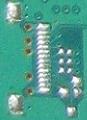
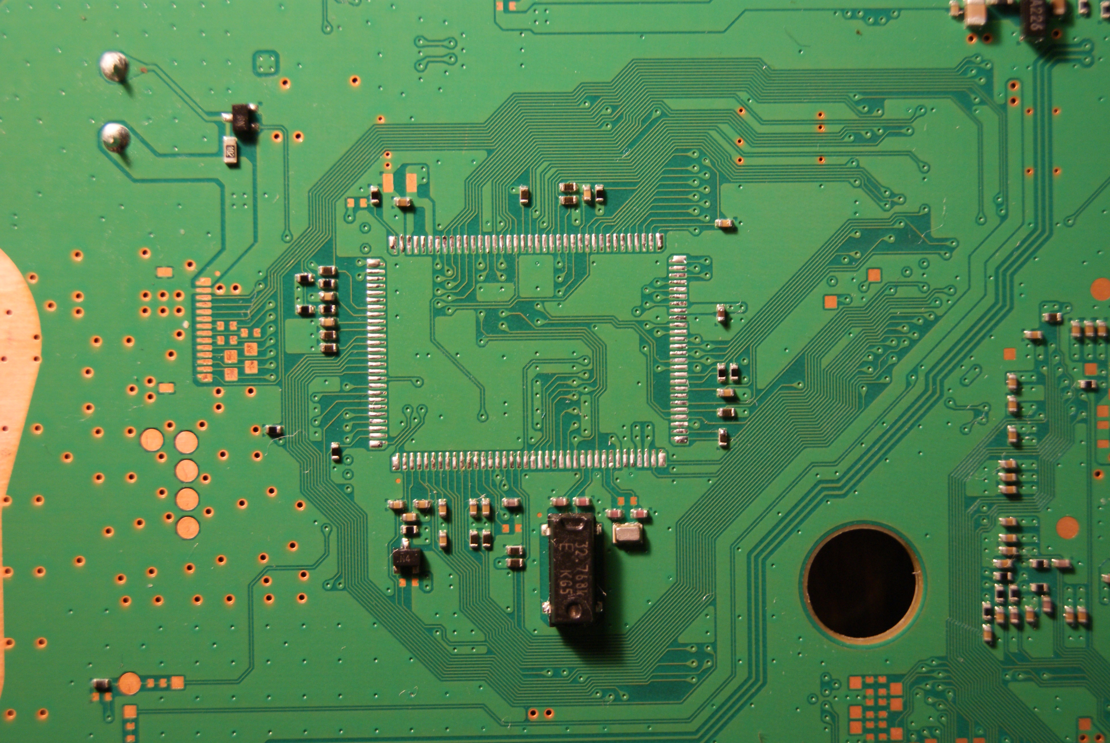
Third Generation Service Connector as seen on VER-001

Third Generation Service Connector as seen on DYN-001

Third Generation Service Connector as seen on DYN-001

Third Generation Service Connector as seen on SURTEES-03
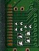
Third Generation Service Connector as seen on JSD-001
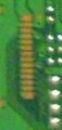
Third Generation Service Connector as seen on MPX-001


CELL_BE_JTAG

Same pinout than previous gen ?
Bluray Drive Diagnostic Port

For pinout see: CN300
Links
https://web.archive.org/web/20160309151818/ http://pastie.org/private/h8osu80ksjr0xdta97zida
https://pastebin.com/hp3Uz6F7 (mirror)
http://docs-asia.electrocomponents.com/webdocs/14a3/0900766b814a341b.pdf
| |||||||||||||||||||||||||||||||||||||||||||||||||||||||||||||||||||||||||||||||||||||||||||||||||||||||||||||||||||||||||||||||||||||||||||||||||||||||||||||||||||||||||||||
