Samsung K8Q2815UQB-PI4B (NOR)
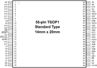
56-pin TSOP1 Standard Type
14mm x 20mm
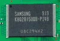
Samsung K8Q2815UQB-PI4B (NOR) as seen on modern PS3 Slim
productcode meaning:
K - Memory
8 - NOR Flash
Q - Small Classification : Page Mode DDP
28 - Density : 128M, 8M / 16Bank / 8^8
15 - Dual Bank Boot Block (Bank1, Bank2) : 16M, 2M / 14M
U - Vcc : 3.0V / 3.3V (2.7V~3.6V)
Q - Device Type: Top and Bottom Boot Block
B - Generation : 3rd Generation
-
P - Package : TSOP1 (Lead Free)
I - Temp : Industrial
4B - Speed : 60ns/25ns (Page)
NOTE
Multiple Bank architectures (8 banks)
- Bank 0 :  8Mbit (4Kw x 8 and 32Kw x 15)
- Bank 1 : 24Mbit (32Kw x 48)
- Bank 2 : 24Mbit (32Kw x 48)
- Bank 3 :  8Mbit (4Kw x 8 and 32Kw x 15)
- Bank 4 :  8Mbit (4Kw x 8 and 32Kw x 15)
- Bank 5 : 24Mbit (32Kw x 48)
- Bank 6 : 24Mbit (32Kw x 48)
- Bank 7 :  8Mbit (4Kw x 8 and 32Kw x 15)
OTP Block : Extra 256 word
- 128word for factory and 128word for customer OTP (only on first Virtual Chip, A22=low)
| Pin |
Usage |
Remarks
|
| 1 |
NC |
No Connection
|
| 2 |
A22 |
Virtual Chip Enable of 2nd Chip
|
| 3 |
A15 |
|
| 4 |
A14 |
|
| 5 |
A13 |
|
| 6 |
A12 |
|
| 7 |
A11 |
|
| 8 |
A10 |
|
| 9 |
A9 |
|
| 10 |
A8 |
|
| 11 |
A19 |
|
| 12 |
A20 |
|
| 13 |
WE |
Write Enable
|
| 14 |
RESET |
Reset
|
| 15 |
A21 |
|
| 16 |
WP/ACC |
Write Protect / Accelerated Program Operation
|
| 17 |
RD/BY |
Ready/Busy Output
|
| 18 |
A18 |
|
| 19 |
A17 |
|
| 20 |
A7 |
|
| 21 |
A6 |
|
| 22 |
A5 |
|
| 23 |
A4 |
|
| 24 |
A3 |
|
| 25 |
A2 |
|
| 26 |
A1 |
|
| 27 |
NC |
No Connection
|
| 28 |
NC |
No Connection
|
| Pin |
Usage |
Remarks
|
| 29 |
VCCQ |
VccQ
|
| 30 |
NC |
No Connection
|
| 31 |
A0 |
|
| 32 |
CE |
Chip Enable
|
| 33 |
VSS |
Ground
|
| 34 |
OE |
Output Enable
|
| 35 |
DQ0 |
|
| 36 |
DQ8 |
|
| 37 |
DQ1 |
|
| 38 |
DQ9 |
|
| 39 |
DQ2 |
|
| 40 |
DQ10 |
|
| 41 |
DQ3 |
|
| 42 |
DQ11 |
|
| 43 |
Vcc |
Vcc (min 2.7V-max 3.6V / typ 3.0V)
|
| 44 |
DQ4 |
|
| 45 |
DQ12 |
|
| 46 |
DQ5 |
|
| 47 |
DQ13 |
|
| 48 |
DQ6 |
*OTP?
|
| 49 |
DQ14 |
|
| 50 |
DQ7 |
*OTP?
|
| 51 |
DQ15 |
|
| 52 |
VSS |
Ground
|
| 53 |
NC |
No Connection
|
| 54 |
A16 |
|
| 55 |
NC |
No Connection
|
| 56 |
NC |
No Connection
|
- OTP Block Region : 256-word Flash memory region. The data DQ6=1 for customer locked and DQ7=1 for factory locked

.jpg)
