Hardware flashing


intro
Before you think this is going to be easy, let me explain why not:
- 18 SKU´s (15 different: CECHAxx · CECHBxx · CECHCxx · CECHExx · CECHGxx · CECHHxx · CECHJxx · CECHKxx · CECHLxx · CECHMxx · CECHPxx · CECHQxx · CECH-20xx · CECH-21xx · CECH-25xx · CECH-30xx · CECH-40xx)
- with 13 different motherboards (COK-001 · COK-002 · COK-002W · SEM-00x · DIA-00x · VER-00x · DYN-00x · SUR-00x · JTP-00x · JSD-00x · KTE-00x · MSX-00x)
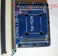
- 9 flashtypes (NAND: Samsung K9F1G08U0A-PIB0 · Samsung K9F1G08U0B-PIB0 · Samsung K9F2G08U0M / NOR: Macronix MX29GL128ELT2I-90G · MX29GL128FLT2I, Samsung K8P2716UZC-QI4D · K8Q2815UQB-PI4B, Spansion S29GL128N90TFIR2 · S29GL128P90TFIR2)
- with 13 different motherboards (COK-001 · COK-002 · COK-002W · SEM-00x · DIA-00x · VER-00x · DYN-00x · SUR-00x · JTP-00x · JSD-00x · KTE-00x · MSX-00x)
- 4 powering options (console powered yes/no, flasher selfpowered yes/no)
- more then 6 hardware flashers (Infectus, Noraliser, NORway' Teensy 2.0++, Progskeet 1.0 / 1.1 / Progskeet 1.2, E3, PNM, PIC32MX)
but even with that amazing number of possible variations, it all comes down to 2 seperate diagrams to use: NAND or NOR.
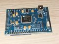
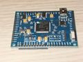
Hardware Flashers
Both early launch consoles which feature NAND flash memory (block devices, that interleave their data unlike NOR flash) and later consoles which feature NOR flash memory are able to be flashed.
Different Flashers
Infectus
...
Noraliser
Marcan has made a NOR flasher / address sniffer for his PS3 slim by re-purposing a FPGA board (Xilinx Spartan3E XC3S500E) made for Wii hacking. Noraliser is a git repo that contains the HDL (verilog) and associated host computer tools for flashing/sniffing. There are ~50 signals to solder.
NORway
Work has been underway to brink a low cost AVR (Atmel 90USB1286) based NOR flasher that is capable of reading and writing on all consoles by defyboy. This was opensourced and further enhanced, now known as NORway for Teensy 2.0++ boards.
Progskeet
Other people haven't been sitting idle either: uf6667 and bmx have developed Progskeet 1.0 / 1.1, based on an Actel A3P125 FPGA for NAND and NOR based consoles (not only PS3, but also useable for Wii and Xbox360). Later followed up by Progskeet 1.2, which was anounced to get an open API. Although highly hyped/marketed as universal flasher, it is not the recommended end user choice: long history of issues, long time between fixes, no clear support path etc.
PNM
"No_One" has developed PNM - The PS3 NOR Manager is a custom board based on a FPGA (Altera Cyclone3 EP3C25) and 2 flash sockets. PNM is capable to handle the basic features like read/dump/update/copy but also to swap (hot swap or cold swap) the NOR used. It also enbles features to sniff bus activities, emulate NOR flash etc.
PIC32MX
PIC32MX is an opensource PIC based NOR flasher.
E3
The E3 is a China commercial developped PS3 only 'flasher'.
It uses MCU ARM 32BIT 256K FLASH 144LQFP - STM32F103ZCT6 controller to dump the NOR.
Comparison
| Flasher | FAT | SLIM | Notes | ||||||||||
|---|---|---|---|---|---|---|---|---|---|---|---|---|---|
| CECHA CECHB |
CECHC CECHE |
CECHE | CECHG | CECHH | CECHK | CECHL CECHM CECHP CECHQ |
CECH-20.. | CECH-21.. | CECH-25.. | CECH-25.. | CECH-30.. | ||
| COK 001 |
COK 002 |
COK 002W |
SEM 001 |
DIA 001 |
DIA 002 |
VER 001 |
DYN 001 |
SUR 001 |
JTP 001 |
JSD 001 |
KTE 001 | ||
| Infectus | Yes | Yes | Yes | Yes | No | No | No | No | No | No | No | No | NAND only |
| Progskeet 1.0 / 1.1 | Issues | Issues | Issues | Issues | Issues | Issues | Issues | Issues | Issues | Issues | Issues | Issues | advertised Universal NAND + NOR + SPI |
| Progskeet 1.2 | Issues | Issues | Issues | Issues | No | No | No | No | No | No | No | No | advertised Universal NAND + NOR + SPI |
| Progskeet 1.21 | Issues | Issues | Issues | Issues | No | No | No | No | No | No | No | No | advertises Universal NAND + NOR + SPI |
| Teensy 2.0++: NANDway / NORway | Yes | Yes | Yes | Yes | Yes | Yes | Yes | Yes | Yes | Yes | Yes | Yes | OpenSource / OpenHardware + works for NAND + NOR |
| PNM | No | No | No | No | Yes | Yes | Yes | Yes | Yes | Yes | Yes | Yes | OpenSource / OpenHardware |
| Noraliser | No | No | No | No | Yes | Yes | Yes | Yes | Yes | Yes | Yes | Yes | Not commercially avail. |
| PIC32MX | No | No | No | No | Yes | Yes | Yes | Yes | Yes | Yes | Yes | Yes | OpenSource / OpenHardware |
| E3 | No | No | No | No | Yes | Yes | Yes | Yes | Yes | Yes | Yes | Yes | 1 console only (unless you use the Samsung multi console update) |
| Feature | Infectus | PNM | Progskeet 1.0 / 1.1 | Progskeet 1.2 / 1.21 | Teensy 2.0++ NANDway / NORway |
PIC32MX | E3 | Remarks |
|---|---|---|---|---|---|---|---|---|
| Use CFI | ? | Yes | Yes | - | No | ? | ? | Common Flash Memory Interface writing strategies (Progkseet can dump CFI, but doesnt use it directly for writestrategy) |
| PS3 NAND Support (see above table) |
Yes | No | Yes | - | Yes | No | Yes | E3 supports NAND with later 'to be released' edition |
| PS3 NOR Support (see above table) |
No | Yes | Yes | - | Yes | Yes | Yes | |
| Solderless | No | No | Yes | - | No | No | Yes | Solderless is optional for E3 (but still requires soldering tristate).
NOR/NAND solderless clip for Progskeet 1.0 / 1.1 are already available now. Announced for PNM near future. |
| OpenSource | No | Yes | No | - | Yes | Yes | No | |
| OpenHardware | No | Yes | No | - | Yes | Yes | No | |
| Updateable | JTAG | USB | JTAG | - | USB | ISP | microSD | |
| Onboard Flash | No | Yes | No | - | No | No | Yes | Instant-on dual firmware for PNM using a jumper // E3 uses flash on driveboard, not internal |
| Dual Boot solution | No | Yes | Yes | - | No | No | Yes | Real quick dualboot requires dual flash (and user to swap the harddrive) |
| File Transfer Protocol | USB | X-Modem | USB | - | USB | |||
| Mass Production | No | No | Yes | - | No | No | Yes | PNM V2 might be mass produced |
| X360 NAND Support | Yes | No | Yes | - | No | No | No | |
| Wii NAND Support | Yes | No | Yes | - | No | No | No |
Generic Warning
| Generic Warning |
|---|
Make sure you have several proper dumps of your flash before even trying writing to it! Use unpacking tools (e.g. Norunpack, Flowrebuilder, Norpatch etc.) and hexeditors (e.g. HxD) and use Flash page as reference.
See also: Validating flash dumps You cannot recover from bad flash without proper dumps (e.g. bricking the console beyond repair). |
NAND Wiring
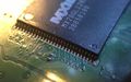
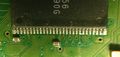
Flashers for NAND based consoles (CECHA/COK-001, CECHB/COK-001, CECHC/COK-002, CECHD/unreleased, CECHE/COK-002W, CECHF/unreleased, CECHG/SEM-001) are generaly wired directly to the pins of the NAND (you cannot use the testpoints!), plus ground and Vcc. For NAND pinouts see: Flash (Hardware) #NAND
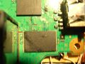
There are 2 nands interleaved at the 512byte sectors level, giving a 1024 byte "interleaved sector". pages are 2kb on each nand.
Which NAND is low (NAND 0)/high (NAND 1)?
- COK-001 :
- IC3802 LOW (main componentside next to Starship2)
- IC3803 HIGH (backside next to 60-pin BD ATA connector)
- COK-002 + COK-002W :
- IC3802 LOW (main componentside between SATA connector and South Bridge)
- IC3803 HIGH (main componentside between SATA connector and AV Multi connector)
- SEM-001 :
- IC3802 LOW (backside)
- IC3803 HIGH (main componentside with SATA connector, CELL BE, RSX etc.)
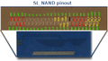
Pinout Table


| Chip/PIN | Description | NANDway | Progskeet 1.0 / 1.1 S-NAND | Progskeet 1.0 / 1.1 SL-NAND | Progskeet 1.2 / 1.21 | Infectus | 360clip | Description |
|---|---|---|---|---|---|---|---|---|
| NAND 0 | ||||||||
| 0/1-6 | NC | NC | NC | NC | NC | NC | NC | No Connection |
| 0/7 | R/B | PB6 | 64 / rdy | gp5 | P02 | U | FRB1 | Read/Busy Output |
| 0/8 | RE | PB1 | 69 / oe | gp1 | P06 | M | RE | Read Enable |
| 0/9 | CE | PB0 | 60 / gp3 | gp2 | P05(p) CE_A / P03(s) CE_B | N | FCE1 | Chip Enable |
| 1/10+11 | NC | NC | NC | NC | NC | NC | NC | No Connection |
| 0/12 | Vcc | +3.3 | +3.3 | +3.3 | NC | Vcc | Vcc (min 2.7V-max 3.6V / typ 3.3V) | |
| 0/13 | Vss | GND | GND | GND | NC | GND | VSS - Ground | |
| 1/14+15 | NC | NC | NC | NC | NC | NC | NC | No Connection |
| 0/16 | CLE | PB2 | 63 / gp0 | we | P09 | O | CLE | Command Latch Enable |
| 0/17 | ALE | PB3 | 62 / gp1 | rdy | P08 | P | ALE | Address Latch Enable |
| 0/18 | WE | PB5 | 65 / we | gp0 | P07 | Q | WE | Write Enable |
| 0/19 | WP | PB4 | 61 / gp2 | gp3 | P04 | T | WP | Write Protect |
| 1/20-28 | NC | NC | NC | NC | NC | NC | NC | No Connection |
| 0/29 | I/O-0 | PF0 | 79 / dq0 | 79 / dq0 | P34 | D0 | I/O0 | |
| 0/30 | I/O-1 | PF1 | 80 / dq1 | 80 / dq1 | P35 | D1 | I/O1 | |
| 0/31 | I/O-2 | PF2 | 81 / dq2 | 81 / dq2 | P36 | D2 | I/O2 | |
| 0/32 | I/O-3 | PF3 | 82 / dq3 | 82 / dq3 | P37 | D3 | I/O3 | |
| 0/33-35 | NC | NC | NC | NC | NC | NC | NC | No Connection |
| 0/36 | Vss | GND | GND | GND | NC | GND | VSS - Ground | |
| 0/37 | Vcc | +3.3 | +3.3 | +3.3 | NC | Vcc | Vcc (min 2.7V-max 3.6V / typ 3.3V) | |
| 0/38-40 | NC | NC | NC | NC | NC | NC | NC | No Connection |
| 0/41 | I/O-4 | PF4 | 83 / dq4 | 83 / dq4 | P38 | D4 | I/O4 | |
| 0/42 | I/O-5 | PF5 | 84 / dq5 | 84 / dq5 | P39 | D5 | I/O5 | |
| 0/43 | I/O-6 | PF6 | 85 / dq6 | 85 / dq6 | P40 | D6 | I/O6 | |
| 0/44 | I/O-7 | PF7 | 86 / dq7 | 86 / dq7 | P41 | D7 | I/O7 | |
| 0/45-48 | NC | NC | NC | NC | NC | NC | NC | No Connection |
| 0/- | NC | NC | NC | NC | NC | NC | PRE | Not used |
| 0/10 | NC | NC | NC | NC | NC | NC | FCE2 | Not used |
| 0/6 | NC | NC | NC | NC | NC | NC | FRB2 | Not used |
| 0/- | NC | NC | NC | NC | NC | NC | RST | Not used |
| NAND 1 | ||||||||
| 1/1-6 | NC | NC | NC | NC | NC | NC | NC | No Connection |
| 1/7 | R/B | PD6 | 3 / gp13 | a15 | P26 | A9 | FRB1 | Read/Busy Output |
| 1/8 | RE | PD1 | 98 / gp15 | a19 | P30 | A15 | RE | Read Enable |
| 1/9 | CE | PD0 | 7 / gp9 | a18 | P29(p) CE_A / P27(s) CE_B | A14 | FCE1 | Chip Enable |
| 1/10+11 | NC | NC | NC | NC | NC | NC | NC | No Connection |
| 1/12 | Vcc | +3.3 | +3.3 | +3.3 | NC | Vcc | Vcc (min 2.7V-max 3.6V / typ 3.3V) | |
| 1/13 | Vss | GND | GND | GND | NC | GND | VSS - Ground | |
| 1/14+15 | NC | NC | NC | NC | NC | NC | NC | No Connection |
| 1/16 | CLE | PD2 | 4 / gp12 | a22 | P33 | A13 | CLE | Command Latch Enable |
| 1/17 | ALE | PD3 | 5 / gp11 | a21 | P32 | A12 | ALE | Address Latch Enable |
| 1/18 | WE | PD5 | 2 / gp14 | a20 | P31 | A11 | WE | Write Enable |
| 1/19 | WP | PD4 | 6 / gp10 | a17 | P28 | A10 | WP | Write Protect |
| 1/20-28 | NC | NC | NC | NC | NC | NC | NC | No Connection |
| 1/- | NC | NC | NC | NC | NC | NC | PRE | Not used |
| 1/10 | NC | NC | NC | NC | NC | NC | FCE2 | Not used |
| 1/6 | NC | NC | NC | NC | NC | NC | FRB2 | Not used |
| 1/- | NC | NC | NC | NC | NC | NC | RST | Not used |
| 1/29 | I/O-0 | PC0 | 90 / dq8 | 90 / dq8 | P42 | A0 | I/O0 | |
| 1/30 | I/O-1 | PC1 | 91 / dq9 | 91 / dq9 | P43 | A1 | I/O1 | |
| 1/31 | I/O-2 | PC2 | 92 / dq10 | 92 / dq10 | P44 | A2 | I/O2 | |
| 1/32 | I/O-3 | PC3 | 93 / dq11 | 93 / dq11 | P45 | A3 | I/O3 | |
| 1/33-35 | NC | NC | NC | NC | NC | NC | NC | No Connection |
| 1/36 | Vss | GND | GND | GND | NC | GND | VSS - Ground | |
| 1/37 | Vcc | +3.3 | +3.3 | +3.3 | NC | Vcc | Vcc (min 2.7V-max 3.6V / typ 3.3V) | |
| 1/38-40 | NC | NC | NC | NC | NC | NC | NC | No Connection |
| 1/41 | I/O-4 | PC4 | 94 / dq12 | 94 / dq12 | P46 | A4 | I/O4 | |
| 1/42 | I/O-5 | PC5 | 95 / dq13 | 95 / dq13 | P47 | A5 | I/O5 | |
| 1/43 | I/O-6 | PC6 | 96 / dq14 | 96 / dq14 | P48 | A6 | I/O6 | |
| 1/44 | I/O-7 | PC7 | 97 / dq15 | 97 / dq15 | P49 | A7 | I/O7 | |
| 1/45-48 | NC | NC | NC | NC | NC | NC | NC | No Connection |
| Board trace / Other | ||||||||
| GND | Vss | NC | NC | NC | NC | GND | NC | VSS - Ground |
| +5VDC | Vcc | NC | NC | NC | NC | 5V | NC | Vcc from TH3401 (CECHA+CECHB/COK-001) Vcc from TH3401 (CECHC+CECHE/COK-002) Vcc from TH3280 (CECHG/SEM-001) |
| TRISTATE | tri | PB7 / PD7 | NC | NC | NC | NC | NC | Tristate pad on EBUS Testpoints |
| Chip/PIN | Description | NANDway | Progskeet 1.0 / 1.1 S-NAND | Progskeet 1.0 / 1.1 SL-NAND | Progskeet 1.2 | Infectus | 360clip | Description |
Remarks:
- Progskeet 1.0 / 1.1 is feeded from NAND 3.3V
- Infectus is feeded from +5V board trace.
- NAND's are feeded in both cases by the console itself.
Progskeet 1.0 / 1.1 Note: Some modification is needed for Progskeet 1.0 / 1.1 to unbrick:
- desolder R8 from the Progskeet 1.0 / 1.1 PCB (to disable the connection from pad R8 to left pad R7)
- left pin of toggle switch to left lead of R7, middle pin of toggle switch to right lead of R7
- Vcc to +3.3 // put toggle switch in "OFF" (right) postion, power on the ps3, put the toggle switch in the "ON"/left position, it will be recognized by the PC, NAND is always on now, do everything as usual.
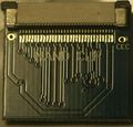
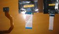
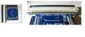
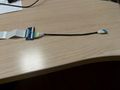
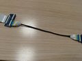
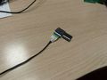
NAND + clips
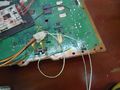
First make sure everything is correct:
- Connect the flasher to the "Y" NAND adapterboard and from there connect the NAND clips to the "Y" NAND adapterboard.
- Install flasher application
- Connect flasher to PC
- Install drivers with zadig.exe (select winusb for latest Winskeet, libusb0 is only for older versions)
- Use the "Check for Shorts" option in the flasherapplication.
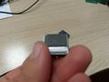
Make sure the clips are fitted correctly over the NANDs:
- note the markerdot for pin1 (both on clip and NAND package)
- make sure all pins make contact
- check if it is all the way down to the PCB evenly and no components surrounding the NAND are preventing it from going down proper (might need some filing to make room).
- You can take the topcap off the clip if you need, and can use hotglue on the outsides to further fixate it.
Preparing console further:
- Replace the thermalcompound (e.g. Arctic Cooling MX-4) for the heatsink : CELL BE and RSX and reassemble the heatsink+fan.
- Connect the Power Supply, Harddrive and the power/resetbutton subboard
- For dumping/reflashing it is not needed to connect the Bluray Drive or the Bluetooth+Wifi board (ofcourse you are going to need them when installing a firmware)
Usage after all is connected:
- First connect flasher to pc
- Use the PS3 to power the NANDs.
Progskeet 1.0 / 1.1 specific:
- On NAND tab, you click NAND 1 and select 'auto'
- On NAND tab, you click NAND 2 and select 'auto'
- If it fails, it means it is not connected correctly
Using NAND flashers
Progskeet 1.0 / 1.1
Method 1 (with R7 switch and R8 closed):
put switch in "OFF" (R7 is open) position so that Progskeet 1.0 / 1.1 is not powered.
power on the ps3 and wait for 10-15 seconds (sometimes shorter time is needed),
put the switch in the "ON" (R7 closed) position, so Progskeet 1.0 / 1.1 is powered and will be recognized by the PC.
NAND is always on now, do everything as usual

select Big Block
select Raw
Pages per block: 64
blocks: 1024

That will give you 132MB (138,412,032 bytes) per NAND (dump time ~ 00:02:40 per NAND)

For normal console operation (e.g. after you dumped, flashed/downgraded it):
you need switch to "on" (R7 closed) and Progskeet 1.0 / 1.1 USB disconnected.
Method 2 (with R7 open / R8 closed):
1. Remove USB cable from your PC
2. Open up Progskeet 1.0 / 1.1 flashing software (use latest) and on Common tab: select the flash you have @ Presets
3. Power on PS3 and wait 10-15 seconds (sometimes shorter time is needed),
4. Plug in the USB cable to your PC
5. Progskeet 1.0 / 1.1 will be recognised and you can now go ahead and dump
For normal console operation (e.g. after you dumped, flashed/downgraded it):
you need to disconnect the USB cable to your PC
downloads
All current downloads are available here / all backup/mirror are here
Infectus
For Infectus don't use 3.9.9.0, as it removes dual NAND PS3 support :S If your board already came with this version or higher, use this: prepare_infectus_for_ps3.rar (5.53 MB) If it is done, it will show up as "2 NAND Programmer" in the bottom left. Dual NAND PS3 compatible version: Infectus_programmer_3.8_Beta_2.zip (4.02 MB)
Power the Infectus, it crashes the PS3 and leaves the NANDs in powered mode. Use the console to power the NANDs: power it up until the PS3 crashes and halts with red flashing LED, press power again to stop the flashing, but keeps the console powered on. The NANDs are not accessed by the PS3 in this way, so it doesn't matter if the NAND content is already messed up. After that, you can read/write the NANDs.
Dumping of single NAND should take about 15 minutes, 30 minutes for both.
Needed NAND tools
In case the flasher program doesnt understand dual NAND de/interleaving you'll need : FlowRebuilder
Flowrebuilder options
- (NAND only) Unscramble then interleave flashes into one unified dump : Makes a single dump.bin from 2 seperate NAND flash dumps.
- In the second step it also extract the content of the unified dump. Make sure it extracts correctly (it will give no warning if it fails!) and all the needed files are there.
- (NAND only) Re-scramble modified dump then de-interleave it into two new flashes : Splits the single dump.bin into 2 seperate NAND flash dumps.
- Byte reverse and extract a NOR dump file : First byte reverse the single dump.bin then extract NOR content.
- Extract a Byte reversed NOR dump or an interleaved and unscrambled NAND dump : Extract the single dump.bin
Extracted flash content files
(make sure they are all there, flowrebuilder will not give warning when it fails!):
- bootloader_0
- bootloader_1
- cCSD
- cISD
- creserved_0
- cvtrm
- eEID
- trvk_pkg
- trvk_prg
- \asecure_loader\metldr
- \ros\[two seperate folders named to FW version]\CoreOS files (19 up to 25 files, depending the FW version)
Notes: if it only extracted bootloader_0 + bootloader_1, check that both NANDs are dumped correct (known error with flashers that has bug with second NAND channel to read),
Dump NAND from GameOS
USB Flash Dump // source/mirror:
dump_flash.pkg
Make sure USB stick is FAT32 with enough free space (256MB per dump)
Dumping NAND from Linux
dd if=/dev/ps3flash of=NAND.BIN bs=1024
or
dd if=/dev/ps3vflasha of=NAND.BIN bs=1024
(needs unmasking first, see below)
Difference between hardware dumps and software dumps
ps3vflasha
hardware dumps
256 MB (268,435,456 bytes) bootldr is at 0x000000 on NAND (0xFC0000 on NOR)
software dumps
dump size = 239 MB (251,396,096 bytes)
bootldr not at 0x000000 on NAND :
00000000 00 00 00 00 00 00 00 00 00 00 00 00 00 00 00 00 ................ 00000010 00 00 00 00 0F AC E0 FF 00 00 00 00 DE AD BE EF .....¬à ÿ....Þ¾ï
reason:
addi %r12, %r4, 0x200 # r4 = start sector
256MB NAND consoles have a hidden section of size 0x40000 (0x200 * 512 byte sector = 0x40000) hidden by the hv. The hv hides it at address 002786E8
Original code : 0x39840200f8010090
Change to : 0x39840000f8010090
as seen in unself'ed LV1.self (Hypervisor)
3.15:
    Offset(h) 00 01 02 03 04 05 06 07 08 09 0A 0B 0C 0D 0E 0F
    00098D20                                      39 84 02 00              9„..
    00098D30  F8 01 00 90                                      ø...
3.41:
    Offset(h) 00 01 02 03 04 05 06 07 08 09 0A 0B 0C 0D 0E 0F
    000986A0  39 84 02 00 F8 01 00 90                          9„..ø...
| Brick warning - Peek/Poke only |
|---|
| #Brick warning
TCL: http://pastebin.com/Snh4ERQ6 (Don't use, BRICK RISK, see below) Too dangerous to patch unless you peek/poke because obviously it messes with all the offsets |
Guide to unbrick from above situation
Here's my guide http://www.mediafire.com/?76bw1vd1m65bkk4 . I haven't tested it yet, but it should work on COK-001
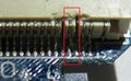
'NOR' Interface Testpoints on NAND consoles
Simular as on the NOR based consoles testpoints can be found on the back of the PCB. It seems these are from the bus between the South Bridge and the Starship2. Attempts have been made to document/trace these. Addresslines 0-17 and Datalines 0-15 as well as some controllines are documented but so far these could not be used to read/flash the console in a NOR fashion.
TriState on NAND consoles
using Starship2 to South Bridge BRDY /SS2_BRDY
- CECHA (COK-001): EBUS jl:9309 (page 20 of servicemanual) / (named BRDY in File:COK-001-NOR_1.jpg)
- CECHC + CECHE (COK-002): EBUS jl:9309 (page 20 of servicemanual)
- CECHG (SEM001): EBUS jl:9309 (page 21 of servicemanual) / (named SB_TRI in File:SEM-001-tristate.jpg)
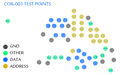
NOR Interface Testpoints
Probably to aid in factory programming, Sony provides NOR testpoints on the bottomside of the motherboard. There are 16 data lines (Word access) and generally 23 Address lines. You will also need to control Chip Enable (#CE), Write Enable (#WE), Tristate (SB_DISABLE) and for some boards Write Protect (#WP)
Tristate
Tristate, or as it is referred to in the service manuals SB_DISABLE exists solely for the purpose of placing the South Bridge pins into high-impedance (the third state) so that we can access the flash without the South Bridge interfering.
Because the tristate pin is not connected to the NOR flash TSOP package, but to the South Bridge BGA package, this makes tracing the pin quite difficult. One should be able to locate it by having the running you could ground out the unknown pins whilst checking the continuity of a known address or data line against ground. These should enter high-impedance or no-continuity when you ground out SB_DISABLE.
Connecting NOR pads to flasher


| NORpin | PAD | Progskeet 1.0 / 1.1 | Progskeet 1.2 | Teensy++ 2.0 NORway |
PNM | E3 / E3 Linker | NOR56 360clip | Remark |
|---|---|---|---|---|---|---|---|---|
| 31 | A0 | adr0 | P11 | F0 | A0 | A0 | FA0 | |
| 26 | A1 | adr1 | P12 | F1 | A1 | A1 | FA1 | |
| 25 | A2 | adr2 | P13 | F2 | A2 | A2 | FA2 | |
| 24 | A3 | adr3 | P14 | F3 | A3 | A3 | FA3 | |
| 23 | A4 | adr4 | P15 | F4 | A4 | A4 | FA4 | |
| 22 | A5 | adr5 | P16 | F5 | A5 | A5 | FA5 | |
| 21 | A6 | adr6 | P17 | F6 | A6 | A6 | FA6 | |
| 20 | A7 | adr7 | P18 | F7 | A7 | A7 | FA7 | |
| 10 | A8 | adr8 | P19 | PA0 | A8 | A8 | FA8 | |
| 9 | A9 | adr9 | P20 | PA1 | A9 | A9 | FA9 | |
| 8 | A10 | adr10 | P21 | PA2 | A10 | A10 | FA10 | |
| 7 | A11 | adr11 | P22 | PA3 | A11 | A11 | FA11 | |
| 6 | A12 | adr12 | P23 | PA4 | A12 | A12 | FA12 | |
| 5 | A13 | adr13 | P24 | PA5 | A13 | A13 | FA13 | |
| 4 | A14 | adr14 | P25 | PA6 | A14 | A14 | FA14 | |
| 3 | A15 | adr15 | P26 | PA7 | A15 | A15 | FA15 | |
| 54 | A16 | adr16 | P27 | B0 | A16 | A16 | FA16 | |
| 19 | A17 | adr17 | P28 | B1 | A17 | A17 | FA17 | |
| 18 | A18 | adr18 | P29 | B2 | A18 | A18 | FA18 | |
| 11 | A19 | adr19 | P30 | B3 | A19 | A19 | FA19 | |
| 12 | A20 | adr20 | P31 | B4 | A20 | A20 | FA20 | |
| 15 | A21 | adr21 | P32 | B5 | A21 | A21 | FA21 | |
| 1 | A23 | Not Used | Not Used | Not Used | Not Used | Not Used | FA23 | pin unused for 128mbit and below |
| 56 | A24 | Not Used | Not Used | Not Used | Not Used | Not Used | FA24 | pin unused for 256mbit and below |
| 2 | A22 | adr22 | P33 | B6 | A22 | A22 | FA22 | |
| 35 | DQ0 | dq0 | P34 | D0 | DQ0 | D0 | AD0 | |
| 37 | DQ1 | dq1 | P35 | D1 | DQ1 | D1 | AD1 | |
| 39 | DQ2 | dq2 | P36 | D2 | DQ2 | D2 | AD2 | |
| 41 | DQ3 | dq3 | P37 | D3 | DQ3 | D3 | AD3 | |
| 44 | DQ4 | dq4 | P38 | D4 | DQ4 | D4 | AD4 | |
| 46 | DQ5 | dq5 | P39 | D5 | DQ5 | D5 | AD5 | |
| 48 | DQ6 | dq6 | P40 | D6 | DQ6 | D6 | AD6 | |
| 50 | DQ7 | dq7 | P41 | D7 | DQ7 | D7 | AD7 | |
| 36 | DQ8 | dq8 | P42 | C0 | DQ8 | D8 | AD8 | |
| 38 | DQ9 | dq9 | P43 | C1 | DQ9 | D9 | AD9 | |
| 40 | DQ10 | dq10 | P44 | C2 | DQ10 | D10 | AD10 | |
| 42 | DQ11 | dq11 | P45 | C3 | DQ11 | D11 | AD11 | |
| 45 | DQ12 | dq12 | P46 | C4 | DQ12 | D12 | AD12 | |
| 47 | DQ13 | dq13 | P47 | C5 | DQ13 | D13 | AD13 | |
| 49 | DQ14 | dq14 | P48 | C6 | DQ14 | D14 | AD14 | |
| 51 | DQ15 | dq15 | P49 | C7 | DQ15 | D15 | AD15 | |
| 13 | #WE | we | P09 | E5 | NWE | NWE | WE | |
| 32 | CE# | gp0 | P07(p) CE_A / P02(s) CE_B | E0 | NCE | CE to NOR (SBCE from South Bridge) |
CE# | |
| 14 | RESET | gp1 | P06 | E4 | NRESET | RESET | RESET | |
| N/A | TRISTATE | gp2 | P05 | E7 | GPIO0 | SBE | N/A | |
| 16 | WP# | gp3 | P04 | Not Used | NWPACC | Not used | WP# | Is tied to Vcc by mobo |
| 53 | BYTE# | Not Used | Not used | Not used | Not used | BVCC | ? | Is tied to Vcc by mobo |
| 34 | OE# | oe | P10 | E1 | NOE | NOE | OE | |
| 17 | RY/BY# | rdy (ánd gp4 for old bitstream) | P08 | E6 | RYNBY | NWAIT | RDY | JTAG updated progskeet can do without the progskeet:gp4 to progskeet:rdy bridge and use the PS3:RY/BY# to progskeet:rdy alone. |
| 33, 52 | VSS | GND | GND | GND | GND | GND | ||
| 29, 43 | VCC | Not Used | Not used | Not used | VCC | ? | ||
| 27, 28, 30, 55 | NC | Not Used | Not Used | Not Used | Not Used | Not Used | Not Used | pins unused / Not Connected |
Progskeet 1.0 / 1.1 notes
Some modification is needed for Progskeet 1.0 / 1.1 to unbrick:
- desolder R8 from the Progskeet 1.0 / 1.1 PCB
- left pin of switch to left lead of R7, middle pin of switch to right lead of R7
- Vcc to +3.3 // put switch in "OFF" (right) postion, power on the ps3, put the switch in the "ON"/left position, it will be recognized by the PC, NOR is always on now, do everything as usual.
PNM notes
- PNM requires a +5V_EVER from the PS3 motherboard in "PS3 mode"
- PNM requires a +5V from a USB port in "standalone mode". It then provides a +3.3V to the embedded NOR.
Teensy notes
- The Teensy requires a 3.3V voltage regulator! 5V trace has to be cut and 3V pads have to be shorted! Please refer to https://www.pjrc.com/teensy/3volt.html
E3 debricking notes
- Requires soldering wire from SBE (solderpad on NOR flatcable) to TRISTATE (NORpoint on PS3 motherboard)
- Make sure you have correct firmware on SD/TF card
- E3 switches set as 1:Flash fun, 2: OFW, 3: Prog, 4: microSD, 5: PS3 Flash, 6: Lock with the console power disconnected.
- Turn on console to restore (progress LEDs will light up one by one and blink if successfully).
- Unplug powercable and set 1:Flash fun down to PS3 Mode and turn on the PS3, if everything went fine, it will now be debricked (remember: in case syscon has 3.56+ hashes, you need prepatched LV1, see downgrader guides).
Speed comparison NOR flashers
| Speed comparison NOR flashers | ||||||||
|---|---|---|---|---|---|---|---|---|
| Teensy 2.0++ (NORway 0.1) |
Teensy 2.0++ (NORway 0.3) |
Progskeet 1.0 / 1.1 | PNM (X-Modem - 460800 baud) | |||||
| time (h:mm:ss) | speed (KB/sec) | time (h:mm:ss) | speed (KB/sec) | time (h:mm:ss) | speed (KB/sec) | time (h:mm:ss) | speed (KB/sec) | |
| Full dump/read (16 MB) | 0:05:11 | 52,68 KB/s | 0:00:45 | 364,08 KB/s | 0:00:16 | 1024 KB/s | 0:45:43 | 6,1 KB/s |
| Per sector write(128 KB) | 0:01:35 | 1,35 KB/s | 0:00:05.351 | 23,92 KB/s | 0:00:00.365 | 350,69 KB/s | 0:00:16.12 | 7,90 KB/s |
| Full dump/write (16 MB) | 2:08:19 | 2,12 KB/s | 0:08:19 | 32,83 KB/s | 0:00:46.811 | 350,00 KB/s | 0:34:56 | 7,90 KB/s |
| Full CRC32 (16 MB) | 0:01:30 | 182,04 KB/s | ||||||
| Full copy NOR-NOR (16 MB) | 0:04:59 | 54,61 KB/s | ||||||
Using NOR flashers
Progskeet 1.0 / 1.1
Method 1 (with R7 switch and R8 closed):
1. Unplug the PS3 powercable from the back
2. Open up Progskeet 1.0 / 1.1 flashing software (use latest) and on Common tab: select the flash you have @ Presets
3. Set the R7 switch to "off"
4. Plug the PS3 powercable back in and Power on the PS3
5. Wait 10 seconds and set the R7 switch to "on" to power Progskeet 1.0 / 1.1 (sometimes shorter time is needed)
6. Progskeet 1.0 / 1.1 will be recognised and you can now go ahead and dump
For normal console operation (e.g. after you dumped, flashed/downgraded it):
you need switch to "on" (R7 closed) and Progskeet 1.0 / 1.1 USB disconnected.
Method 2 (with R7 open / R8 closed):
1. Remove USB cable from your PC
2. Open up Progskeet 1.0 / 1.1 flashing software (use latest) and on Common tab: select the flash you have @ Presets
3. Power on PS3 and wait 10 seconds (sometimes shorter time is needed)
4. Plug in the USB cable to your PC
5. Progskeet 1.0 / 1.1 will be recognised and you can now go ahead and dump
For normal console operation (e.g. after you dumped, flashed/downgraded it):
you need to disconnect the USB cable to your PC
NORway
Usage: %s serialport [command] [filename] [address]

serialport  Name of serial port to open (eg. COM1, COM2, /dev/ttyACM0, etc)
command     dump       Reads entire NOR to [filename]
            erase      Erases one sector (128KB) at [address]
            write      Flashes (read-erase-modify-write-verify) [filename]
                       at [address] to NOR
            writeimg   Same as write, but prepend a 16-byte length header
                       [address] is required
            program    Flashes (erase-write-verify) [filename]
                       at [address] to NOR
            release    Releases NOR interface, so the PS3 can boot
filename    Filename for [dump|write|writeimg|program]
address     Address for [erase|write|writeimg|program]
            Default is 0x0, address must be aligned (multiple of 0x20000)
PNM
serialport  (COM1, COM2, etc) - 460800 baud - 8N1
X-Modem protocol for file transfers

            copy_memory             Copies entire NOR to another NOR
            read_memory             Reads 0x80 bytes from a specified offset
            dump_memory             Reads entire NOR to a file (byte swap "on the fly")
            update_memory           Flashes entire NOR from a file (byte swap "on the fly")
            display_memory_crc      Displays NOR CRC32
            display_memory_details  Displays NOR details (size, firmware version, etc)

PNM uses the Common Flash Interface standard (almost all current flash can be dumped/updated)
Needed NOR tools
- norunpack (usage: norunpack dump.b directory) git: http://git.dashhacks.com/ps3free/ps3tools
- FlowRebuilder v.4.2.0.1.rar (379.34 KB)
If your dump starts like this: http://pastebin.com/sS69Vhvf you'll need to use the option "¨Byte reverse and extract a NOR dump file" of Flowrebuilder, which will output a inputfile.REV file
Dump NOR from GameOS
dump_flash.pkg // backup/mirror: dump_flash.pkg (70.48 KB)
Make sure USB stick is FAT32 with enough free space (16MB per dump)
Note: This application takes about 120 minutes to complete the dump, tested on a PS3 80GB CECHL04
Dumping NOR from Linux
dd if=/dev/ps3nflasha of=NOR.BIN bs=1024
Board Revisions
For overview of used types, see flashtypes table
NAND boards - COK-001, COK-002, COK-002W, SEM-001
These are the earliest revisions of the PS3 motherboards: CECHA/COK-001, CECHB/COK-001, CECHC/COK-002, CECHE/COK-002W, CECHG/SEM-001 and contain 2x NAND chips for a total of 256MB. These chips are interleaved which is controlled by a proprietary controller chip codenamed "Starship2" or SS2. This chip handles the interleaving and presents the NAND Chips to the South Bridge as a single large coherent flash over a proprietary EBUS.
Wiring: direct to NAND flash or using boardtraces to NANDs - don't use the testpoints.
NOR layout1 - DIA-001, DIA-002
DIA-001: These boards were the first to get single NOR flash] memory from the middle revisions of the PS3: CECHH/DIA-001, CECHK/DIA-002. Only a single 16MB NOR flash chip is used and the Starship2 chip has been completely removed. The 128N is JEDEC CFI compliant and organized as 8,388,608 words or 16,777,216 bytes, addressable as 16-bit words (PS3 modus operandi) and 8-bit / 1 byte when the BYTE# signal is logic zero.
DIA-002: the pinout is same as DIA-001, the only difference is that DIA-002 doesnt have a WP# testpoint but since it's connected to VCC it is not needed.
NOR layout2 - VER-001
Used in the last revisions of the fatter model PS3 (CECHL, CECHM, CECHP, CECHQ). Single 16MB NOR.
NOR layout3 - DYN-001
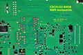
Used in CECH-20xx. The Progskeet 1.0 / 1.1 and teensy pinouts match the teensy picture provided on this page even though it states it's the pinout for Progskeet 1.0 / 1.1. Single 16MB NOR.
NOR layout4 - SUR-001, JTP-001, JSD-001, KTE-001
SUR-001: Used in CECH-21xx. Some difference in components but the testpoints are the same for SUR-001, JTP-001, JSD-001, KTE-001
JTP-001: Used in CECH-25xx. Some difference in components but the testpoints are the same for SUR-001, JTP-001, JSD-001, KTE-001
JSD-001: This is the pinout originally supplied by Marcan for a CECH-2504A. Some difference in components but the testpoints are the same for SUR-001, JTP-001, JSD-001, KTE-001
KTE-001: Used in CECH-30xx. Some difference in components but the testpoints are the same for SUR-001, JTP-001, JSD-001, KTE-001
NOR layout5 - MSX-001 and MPX-001
MSX-001 and MPX-001: Used in CECH-40xx. Much difference in components positioning (main hearth of the board is 45 degrees rotated), but it still has testpoints.
Gallery
Pinout Gallery
NAND
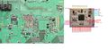
Starship2 EBUS Testpoints (NAND board) do not use!
COK-001 EBUS Testpoints (NAND board - only overlay) do not use!

COK-001 EBUS Testpoints (NAND board) do not use!
COK-002 EBUS Testpoints (NAND board) do not use!
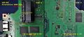
COK-002 - NANDs
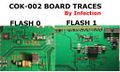
COK-002 boardtraces (NAND board) needs Testing/Confirmation (incomplete: 3 points still missing)
SEM-001 boardtraces (NAND board)
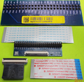
Progskeet - Single NAND - 360clip
NAND TSOP48 360clip (note: no need to connect R/B2 on ps3's)
Progskeet SL-NAND adaptorboard
1Gbit NANDclip - Front
1Gbit NANDclip - Back


NOR
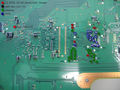
DIA-001 NOR Testpoints (NOR layout 1)
DIA-002 NOR Testpoints (NOR layout 1)
VER-001 NOR Testpoints (NOR layout 2)
VER-001 NOR Testpoints - trisaster.de, missing Tristate (NOR layout 2)
DYN-001 NOR Testpoints (NOR layout 3)
DYN-001 NOR Testpoints + dualboot 'AB mod' (NOR layout 3)
DYN-001 NOR Testpoints with progskeet labeling (NOR layout 3)
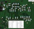
JSD-001, JTP-001, KTE-001 NOR Testpoints with Progskeet labeling (NOR layout 4)
JSD-001, JTP-001, KTE-001 NOR Testpoints with Progskeet 1.2 labeling (NOR layout 4)
JSD-001 NOR Testpoints (NOR layout 4)
JSD-001 Testpoints - orig. marcan/noraliser (NOR layout 4)
- JTP-001 - 1-882-481-21-testpoints.jpg
JTP-001 NOR Testpoints - not mapped (NOR layout 4)
JTP-001 NOR Testpoints - not mapped (NOR layout 4)
SUR-001 Nor Testpoints - not mapped (NOR layout 4)
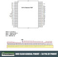
NOR Flash general pinout + 50pin ZIF pinout (Progskeet)
NOR TSOP56 ZIF 360clip and solderboard (Progskeet)
MSX-001 NOR Testpoints - not mapped (NOR layout 5)


Other Gallery
360Clip NAND rework
360Clip NAND SMD why rework
360Clip NOR can't be used for VER-001: no space
360Clip modification pin 48
CLIP comparison
CLIP styles
COK-002 Nand1 SMD components Clip rework
Cutting pin46 360clip-nor - TOPVIEW
Cutting pin48 and 46 360clip-nor
Ext PSU on PS3

Progskeet - NAND-Adaptor PCB (red)
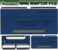
Progskeet - NAND-Adaptor PCB
Damaged NOR. The pins are bent to the shape of the opposing pins on the E3 clip.
Above view of damaged NOR.


Progskeet 1.0 / 1.1 NAND Picture Guide
Full guide is here: Progskeet 1.0 / 1.1
Before
After (R7/R8 + R9/R11 closed)
connect 50pin flatcable
connect Y-subboard
connect NAND flatcable to Y-subboard
connect clip to NAND flatcable
clip + NAND board
NAND board
connect to PC


Generic reference
Torx / Security Bits
- http://microcenter.com/product/208022/33-Piece_Security_Bit_Set
- or if you don't have those, use a smaller flat screwdriver, or just remove the center pin.
Soldering Guide(s)
- http://www.circuitrework.com/guides/7-1-1.shtml
- http://store.curiousinventor.com/guides/Surface_Mount_Soldering/101
- http://en.wikipedia.org/wiki/Desoldering
- http://www.youtube.com/watch?v=E3OmchO_mDc
- http://www.youtube.com/watch?v=SSJGnDHKFQ8
Soldering Irons/Stations
- Soldering Iron
- http://www.amazon.com/Weller-WM120-120v-Pencil-Soldering/dp/B0000WT586/ (good quality/brand)
- http://www.amazon.com/Coopertools-SP12-Mini-Lightweight-Solder/dp/B00002N7S9/ (low budget variant)
- Classic Station
- http://www.amazon.com/Weller-WES51-Analog-Soldering-Station/dp/B000BRC2XU (good quality/brand)
- http://www.amazon.com/Stahl-Tools-Variable-Temperature-Soldering/dp/B0029N70WM/ (lowest budget variant)
- Hot Air Station
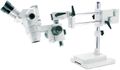
Stereo Microscopes
Things to look for:
- Good solid mounting
- More overhang to reach large boards
- Ring macrolight
- optional: T2 or otherwise adaptor for cameras

Stereo Microscope - example 1
Stereo Microscope - example 2
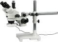
Stereo Microscope - example 3
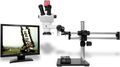
Stereo Microscope - example 4


Tip: also available used
Soldering tips
- Don't use >40W iron (we are not soldering copper pipes!)
- Don't use leadfree solder (232'C @ SnSb)
- Don't use silverbased solder
- Don't use high tin alloy (e.g. 90/10: 300'C @ 97Sn 3Pb and 250'C @ 65Sn 35Pb)
- Use 60/40 (374'F / 190'C) or 63/37 (364'F / 183'C) both have nice low melting point for PCBs
large list of solder alloys and meltingpoints: http://alasir.com/reference/solder_alloys/
Wire reference
For wiring, use 20-26 AWG. 18 can be too stiff while 28 is too fragile. 24-26 AWG works fine in most cases. The Grounds and VCC wires may ofcourse be thicker than the signal wires. Keep wires short, up to ~20cm max (longer gives errors). The shorter the better : 15cm and shorter mostly works fine with AWG26 on NOR.
For NOR wiring the solderarea (the NORpoints) is 10x larger than the solderarea used with NAND (pitch 0.5mm, just as NOR chips btw), so for NOR you have much more headroom (and also need!) to use thicker wires (for NAND you most likely want to use 28 AWG and cannot use much thicker)
Use caliper to measure unknown/unmarked wires and compare with table/listing.
Table: AWG (inch) / Euro (mm)
| American Wire Gauge |
Diameter | Cross Sectional Area |
Diameter | Cross Sectional Area |
Notes |
|---|---|---|---|---|---|
| (AWG) | d (inch) | A (inch2) | d (mm) | A (mm2) | |
| 0000 (-3) | 0,4600 | 0,1662 | 11,6839 | 107,2172 | |
| 000 (-2) | 0,4096 | 0,1318 | 10,4048 | 85,0279 | |
| 00 (-1) | 0,3648 | 0,1045 | 9,2658 | 67,4308 | |
| 0 | 0,3249 | 0,0829 | 8,2515 | 53,4756 | |
| 1 | 0,2893 | 0,0657 | 7,3482 | 42,4085 | |
| 2 | 0,2576 | 0,0521 | 6,5438 | 33,6318 | |
| 3 | 0,2294 | 0,0413 | 5,8275 | 26,6715 | |
| 4 | 0,2043 | 0,0328 | 5,1895 | 21,1516 | |
| 5 | 0,1819 | 0,0260 | 4,6214 | 16,7742 | |
| 6 | 0,1620 | 0,0206 | 4,1155 | 13,3027 | |
| 7 | 0,1443 | 0,0164 | 3,6650 | 10,5496 | |
| 8 | 0,1285 | 0,0130 | 3,2638 | 8,3663 | |
| 9 | 0,1144 | 0,0103 | 2,9065 | 6,6348 | |
| 10 | 0,1019 | 0,0082 | 2,5883 | 5,2617 | |
| 11 | 0,0907 | 0,0065 | 2,3050 | 4,1728 | |
| 12 | 0,0808 | 0,0051 | 2,0527 | 3,3092 | |
| 13 | 0,0720 | 0,0041 | 1,8279 | 2,6243 | |
| 14 | 0,0641 | 0,0032 | 1,6278 | 2,0812 | |
| 15 | 0,0571 | 0,0026 | 1,4496 | 1,6505 | |
| 16 | 0,0508 | 0,0020 | 1,2910 | 1,3089 | |
| 17 | 0,0453 | 0,0016 | 1,1496 | 1,0380 | |
| 18 | 0,0403 | 0,0013 | 1,0238 | 0,8232 | |
| 19 | 0,0359 | 0,0010 | 0,9117 | 0,6528 | |
| 20 | 0,0320 | 0,0008 | 0,8119 | 0,5177 | |
| 21 | 0,0285 | 0,0006 | 0,7230 | 0,4106 | |
| 22 | 0,0253 | 0,0005 | 0,6439 | 0,3256 | |
| 23 | 0,0226 | 0,0004 | 0,5734 | 0,2582 | |
| 24 | 0,0201 | 0,0003 | 0,5106 | 0,2048 | |
| 25 | 0,0179 | 0,0003 | 0,4547 | 0,1624 | |
| 26 | 0,0159 | 0,0002 | 0,4049 | 0,1288 | Best used for NOR consoles |
| 27 | 0,0142 | 0,0002 | 0,3606 | 0,1021 | |
| 28 | 0,0126 | 0,0001 | 0,3211 | 0,0810 | Best used for NAND consoles |
| 29 | 0.0113 | 0.286 | 0.064 | ||
| 30 | 0.0100 | 0.255 | 0.051 | ||
| 31 | 0.00893 | 0.227 | 0.040 | ||
| 32 | 0.00795 | 0.202 | 0.032 | ||
| 33 | 0.00708 | 0.180 | 0.025 | ||
| 34 | 0.00631 | 0.160 | 0.020 | ||
| 35 | 0.00562 | 0.143 | 0.016 | ||
| 36 | 0.00500 | 0.127 | 0.013 | ||
| 37 | 0.00445 | 0.113 | 0.010 | ||
| 38 | 0.00397 | 0.101 | 0.008 | ||
| 39 | 0.00353 | 0.0897 | 0.006 | ||
| 40 | 0.00314 | 0.0799 | 0.005 |
Alternative/cable comparison
   PATA/floppy 40-conductor cable - AWG28 (0.0126" / 0.321mm) with 0.0333" pitch +/- 0.002"
   PATA/floppy 40-conductor cable - AWG30 (0.0100" / 0.255mm) with 0.0333" pitch +/- 0.002"

   PATA 80-conductor cable - AWG30 (0.0100" / 0.255mm) with 0.025" pitch +/- 0.0016"
   PATA 80-conductor cable - AWG30 (0.0100" / 0.255mm) with 0.025" pitch +/- 0.002"
   PATA 80-conductor cable - AWG31 (0.00893" / 0.227mm) with 0.025" pitch +/- 0.002"
   PATA 80-conductor cable - AWG32 (0.00795" / 0.202mm) with 0.025" pitch +/- 0.002"

   Category 6 (ANSI/TIA-568-B.2-1) network cable: 4 twisted pairs of 22AWG (0.0253" / 0.644mm)
   Category 6 (ANSI/TIA-568-B.2-1) network cable: 4 twisted pairs of 23AWG (0.0226" / 0.573mm)
   Category 6 (ANSI/TIA-568-B.2-1) network cable: 4 twisted pairs of 24AWG (0.0201" / 0.511mm)

   Category 5/5e (TIA/EIA 568-5-A) network cable: 4 twisted pairs of 24AWG (0.0201" / 0.511mm)

   Category 5e patch (TIA/EIA 568-5-A) network cable: 4 twisted pairs of 26AWG (0.0159" / 0.405mm)

   SATA : solid 26 AWG - 0.0159" / 0.405mm
   SATA : solid 28 AWG - 0.0126" / 0.321mm
   SATA : solid 30 AWG - 0.0100" / 0.255mm
Generic unresolved issues
There is a table made on the talk page to chart dump/flashing issues (and sucesses). See: Testreport_table
Progskeet 1.0 / 1.1 QA/problem solving
Generic advice
Updating Progskeet 1.0 / 1.1 with Injectus
- connect injectus to Progskeet 1.0 / 1.1with very short wires (see File:Injectus_jtag_pinout.jpg File:Injectus-jtag-bottompads.png)
- power injectus with usb
- power Progskeet 1.0 / 1.1 with its own usb too (do NOT power the Progskeet 1.0 / 1.1 with the injectus!)
- run injectus programmer software
- click tools
- open infectus (at bottom of pulldown)
- load dat file
- click program
See also Programming the Bitstream
R7 / R8 explaination
R7 / R8 explaination in a sketch: File:Progskeet-R7-R8 explaination-sketch4.jpg
Be up to date
Always make sure you used the latest diagrams, drivers and flasher software from progskeet.com
Archive of old versions
Main folder: on ps3devwiki/files
Diagrams
Driver
WinSkeet 111004 and older : use libusb0    Winskeet 111120 and newer: use WinUSB
zadig can be used as driver selector for both, make sure you select the right one.
- drivers_110726.rar (235.62 KB)
- drivers_110812.rar (264.07 KB))
- drivers_a110812.rar (267.61 KB)
- zadig.rar (4,9MB)
Bitstream
- ProgSkeet_Bitstreams_111106.rar (1.63 MB) (NOR solderless and NOR+NAND soldered) Mirror
- ProgSkeet_Bitstreams_111126.rar (1.63 MB) (NAND solderless only) Mirror
Flasher
- ProgSkeet_110803.rar (28.37 KB)
- ProgSkeet_110807.rar (29.24 KB)
- ProgSkeet_110811-A.rar (30.02 KB)
- ProgSkeet_110811-B.rar (29.8 KB)
- ProgSkeet_110812-A.rar (30KB)
- ProgSkeet_110816.rar (32KB)
- ProgSkeet_110819.rar (32.27 KB)
- 111004/8:
- 111120:
- 111205:
- Winskeet111205.rar (4.18 MB) (WinUSB)
No shorts
Before doing anything, make 100% sure you wired up everything correct (no address/data IO lines mixed? all controllines hooked up? power/ground in order? etc.) and no shorts are made where there should not.
Error : libusb0.dll or libusb0.sys not found
The libusb-win32 Kernel Driver needed for the the flasher to get access to the USB port was not installed. Make sure you unpacked the drivers_xxxxxx file and installed the Progskeet driver (VendorID:1988 / ProductID:0001 in case you need it).
If problems with installing the driver, use manual mode from Device Manager and select the folder with ProgSkeet.inf ("ProgSkeet Install Disk") : http://windows.microsoft.com/en-US/windows-vista/Update-a-driver-for-hardware-that-isnt-working-properly
Error : side-by-side configuration is incorrect
In case of "the application has failed to start because its side-by-side configuration is incorrect" make sure Microsoft Visual C 9.0 runtime is installed and "Windows Installer" is not disabled (set to manual or automatic) in Services.msc
Error : incorrect parameter
Make sure you selected the correct values for your NOR/NAND device. If there is a preset, use it
- on Common tab: select the flash you have @ Presets
If not, e.g. :
- NOR
- Spansion S29GL128N90TFIR2 : 128KB sector, 128 sectors
- Spansion S29GL128P90TFIR2 : 128KB sector, 128 sectors
- Samsung K8Q2815UQB-PI4B : 4KB sector, 4096 sectors
- Samsung K8P2716UZC-QI4D : 128KB sector, 128 sectors
- Macronix MX29GL128ELT2I-90G : 128KB sector, 128 sectors
- NAND: select Big Block, select Raw, Pages per block: 64, blocks: 1024
The application failed to initalize properly (0xc0000135)
You are missing either of these:
- http://www.microsoft.com/download/en/details.aspx?displaylang=en&id=29
- http://www.microsoft.com/download/en/details.aspx?id=5582
Error/crash on Windows 7 (and halting on 0x0)
- Disable Aero (known to crash on Win7 Ultimate)
- set display color to 256 colors will enforce Aero to disable too
- Make sure you have enough (admin) rights
- Consider disabling UAC (or re-educate it proper)
- Try "Compatibility Mode" (e.g. Windows 2000 or Windows XP SP2)
Conclusion: 32bit mostly seem to work fine. 64-bit seems tricky/hairy to get working sometimes. Try on good ol' Windows XP 32bit or Linux/OSX to rule out 64bit/chipset responsible for problems.
Timing switching trick
Finally, after many struggles, the way to flash any NOR chip is discovered. Now, here's the method:
- First of all note that when R7 is short - Progskeet 1.0 / 1.1 takes supply from console itself, and when R8 is short - it is powered from USB. So then, whatever you'll do - make sure both R7 and R8 never shorted while console is powered on - this results in damaging mobo as well as console itself.
Preparations are the following: Progskeet 1.0 / 1.1 soldered up correctly, no shorts or testpoints missing; Both R7 and R8 opened. (From now on, just forget about R8) Open Winskeet (Yaskeet, whatever else you got there), set up NOR type and switch to NOR menu. Connect Progskeet 1.0 / 1.1 to PC, power up console. Wait at least 10 seconds then short R7 - Progskeet 1.0 / 1.1 gets recognized by PC. Set up the following options - Single word programming, Static Timing. Now you're ready. Dump NOR several times, check it closely just to be sure it's correct. Prepare patched one then go ahead and write it back to NOR. Though it takes a little longer with mentioned settings, you'll be able to flash it almost correctly. At this point, look out for verification errors - there will be some with almost every NOR I've deal with. The key is that before flashing Progskeet 1.0 / 1.1 reads the NOR and flash only those blocks that differs from desired file. Now, here's the trick itself - after flash process performed with several verification errors, flash back the same file again and again (up to 16 times in a row in several cases), untill number of errors reduces to minimum (three or four). At this point, writing the flash under these settings won't make any changes - this last "hard blocks" will always fail for verification, so just switch to USB Transfer Timing and flash it again. It will take your time around 2 minutes to flash every single block, but since their number were heavily reduced with previous actions, it won't take long in the end. Notice that no verification errors are occured. Now you're done, congratulations)
A/B Trick
The A/B trick is a solution found by DiGiTaLAnGeL to write his Macronix NOR (but can be tried on other NORs as well 1).
Some Sectors of his flash were "slow to write" and using the normal flashing procedure was resulting in a fail or in a freeze of the Progskeet 1.0 / 1.1 Flasher.
Needed tools:
- Download Progskeet Flasher v110811-A // backup/mirror: ProgSkeet_110811-A.rar (30.02 KB)
- Download Progskeet Flasher v110811-B // backup/mirror: ProgSkeet_110811-B.rar (29.79 KB)
Step by step guide:
- Shut Down your PS3 if not and be sure that the Progskeet 1.0 / 1.1 USB Cable is not plugged in.
- Put your R7 Switch in OFF Position.
- Power on your PS3.
- Wait 20 seconds.
- Put your R7 Switch in ON Position (now Proskeet is recognized by Windows).
- Open Flasher "A" and flash your file (remember to set up the NOR size/sectors!)
- When it reaches 100% , check C:\Proskeet.log, if you found some sectors failed to write... continue to the next step.
- Without powering off your PS3, unplug Progskeet 1.0 / 1.1 USB Cable and Close Flasher "A"
- Open Flasher "B" and replug your USB Cable.
- Flash your file (remember to set up the NOR size/sectors!)
- The Flasher will freeze on those "slow" sectors, just wait!
- If after 1 minute your flasher is still stuck on that sector close the flasher.
- Check again your log for sectors failed to write.
If you still have sectors that have failed to write, start again until they successfully write (Rember to check the Progskeet.log because reaching 100% doesn't mean that the sectors have successfully been written)
- note: 1)
- <DiGiAnGeL> if you successfully write at least one of the sectors you are having problem with, this trick work for you!
<DiGiAnGeL> (some sectors require even 5 minutes of trying before successfully writing them)
- <DiGiAnGeL> if you successfully write at least one of the sectors you are having problem with, this trick work for you!
Irregular device disappering when reading/writing
<MrGBNC> I've had good dumps but sometimes when I click read Progskeet 1.0 / 1.1 disappears from the Device Manager
<eussNL> hmm, sounds like voltage drop or usb connection fail
<MrGBNC> and last week was Progskeet 1.0 / 1.1 no longer recognized by windows
<MrGBNC> unknown device
<Abkarino> you may have gnd problem
<eussNL> did you try manual removing the driver in safemode?
<Abkarino> try to remove r4 then try again
<Abkarino> i had the same problem before
<Abkarino> but uf6667 and ago told me to remove r4 and try again
<Abkarino> now Progskeet 1.0 / 1.1 work fine every time i plug it to my PC
<MrGBNC> I've also talked to Ago, he said that the resistance between GND and VCC is too small for my Progskeet 1.0 / 1.1
<Ago> well, you had voltage drops
<Ago> and a cap might be bad
<MrGBNC> that is why I try to exchange/warranty. I also couldn´t read a socket´ed NAND, only 30 in dump ;)