D5305: Difference between revisions
Jump to navigation
Jump to search
m (Added pinout template placeholder for 28nm RSX) |
mNo edit summary |
||
| Line 4: | Line 4: | ||
28nm variants: [[D5305A]] · [[D5305B]] · [[D5305C]] · [[D5305F]] · [[D5305K]] · [[D5305L]] | 28nm variants: [[D5305A]] · [[D5305B]] · [[D5305C]] · [[D5305F]] · [[D5305K]] · [[D5305L]] | ||
{{RSX pad layout 34x34}} | {{RSX pad layout 34x34}} | ||
{{Motherboard Components}}<noinclude>[[Category:Main]]</noinclude> | {{Motherboard Components}}<noinclude>[[Category:Main]]</noinclude> | ||
Revision as of 03:52, 27 June 2021
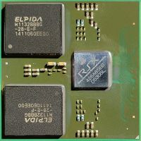
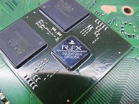
D5305 (RSX - 28nm)


28nm variants: D5305A · D5305B · D5305C · D5305F · D5305K · D5305L
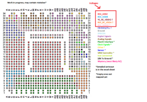
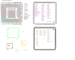
Pinout


RSX D5305 pinout attempt by tracing copper tracks

RSX D5305 pinout and related components based on a NPX-001 board

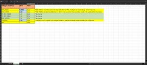
RSX D5305 vs CXD2971GB voltages
| |||||||||||||||||||||||||||||||||||||||||||||||||||||||||||||||||||||||||||||||||||||||||||||||||||||||||||||||||||||||||||||||||||||||||||||||||||||||||||||||||||||||||||||
