D5305: Difference between revisions
Jump to navigation
Jump to search
No edit summary |
|||
| (6 intermediate revisions by one other user not shown) | |||
| Line 1: | Line 1: | ||
== D5305 ([[RSX]] - 28nm) == | == D5305 ([[RSX]] - 28nm) == | ||
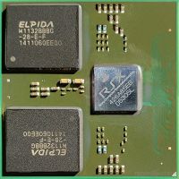
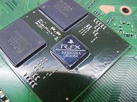
<div style="float:right" | <div style="float:right">[[File:RSX D5305L with elpida W1132BBBG in CECH-43xx REX-001.jpg|200px|thumb|left|[[RSX]] [[D5305]]'''L''' with elpida [[W1132BBBG-28-E-F]] memory in [[CECH-43xx]] [[REX-001]]]]<br>[[File:RSX D5305K with elpida W1132BBBG in CECH-4207B PQX-001.jpg|200px|thumb|left|[[RSX]] [[D5305]]'''K''' with elpida [[W1132BBBG-28-E-F]] memory in [[CECH-42xx]] [[PQX-001]]]]</div> | ||
28nm variants: [[D5305A]] · [[D5305B]] · [[D5305C]] · [[D5305F]] · [[D5305J]] · [[D5305K]] · [[D5305L]] | |||
{{RSX pad layout 34x34}} | |||
{{Motherboard Components}}<noinclude>[[Category:Main]]</noinclude> | {{Motherboard Components}}<noinclude>[[Category:Main]]</noinclude> | ||
Revision as of 12:14, 11 February 2023
D5305 (RSX - 28nm)


28nm variants: D5305A · D5305B · D5305C · D5305F · D5305J · D5305K · D5305L
Pinout


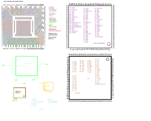
RSX D5305 pinout attempt by tracing copper tracks

RSX D5305 pinout and related components based on a NPX-001 board

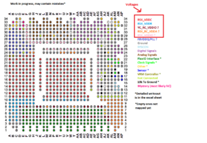
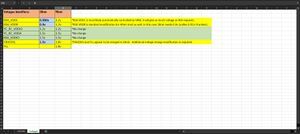
RSX D5305 vs CXD2971GB voltages
| |||||||||||||||||||||||||||||||||||||||||||||||||||||||||||||||||||||||||||||||||||||||||||||||||||||||||||||||||||||||||||||||||||||||||||||||||||||||||||||||||||||||||||||
