CELL BE


Cell Broadband Engine
The Cell CPU has one 3.2Ghz PPE (Power Processor Element) with two threads and eight 3.2Ghz SPE (Synergistic Processing Elements).
The PPE is a general purpose CPU, while the eight SPE are geared towards processing data in parallel. One SPE is disabled to increase yield, so the PS3 can have at most 9 threads running at the same time (2 from PPE and 7 from SPE). Note that one SPE is reserved for the hypervisor, so PS3 programs can take advantage of 8 threads. Both the PPE and SPE of the Cell are 64 bit, and manipulate data in Big Endian.
Specifications
- 1 PPE (Power Processor Element)
- 3.2Ghz
- 64 bit, Big Endian
- 2 threads (can run at same time)
- L1 cache: 32kB data + 32kB instruction
- L2 cache: 512kB
- Memory bus width: 64bit (serial)
- VMX (Altivec) instruction set support
- Full IEEE-754 compliant
- the PPU can execute two double precision or eight single precision operations per clockcycle
- 8 SPE (Synergistic Processing Element)
- 3.2Ghz
- 64 bit, Big Endian
- 1 SPE disabled to improve chip yield (see: Unlocking the 8th SPE)
- 1 SPE dedicated for hypervisor security
- 256KB local store per SPE
- 128 registers per SPE
- Dual Issue (Each SPE can execute 2 instructions per clock)
- IEEE-754 compliant in double precision (single precision round-towards-zero instead of round-towards-even)
There is a lot of info about CELL/BE on the Cell Programming IBM page.
Die explained
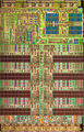
Cell Broadband Engine
Die - 90nm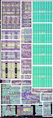
Cell Broadband Engine
SPU Die map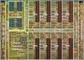
Cell Broadband Engine
Die map - 90nm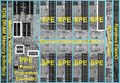
Cell Broadband Engine
Die map - 65nm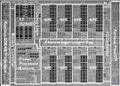
Cell Broadband Engine
Die map - 45nm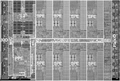
Cell Broadband Engine
Die map - 90nm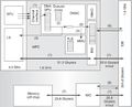
Cell Broadband Engine
SPU diagram


| ABBR | Usage | Speed | Notes |
|---|---|---|---|
| BEI | Broadband engine interface | 1.6GHz (NCLK/2) | I/O Controller to FlexIO(/RSX) |
| EIB | Element interconnect bus | 1.6GHz (NCLK/2) | used as communication ring for the 8 SPE (and PPU + MIC + BEI) |
| FlexIO | High-speed I/O interface | 2.5Ghz (RC_REFCLK : 500MHz 1:5 PLL) | Flex I/O to RSX |
| L2 | Level 2 cache | 3.2GHz (NCLK) | 512KB L2 cache for PPE |
| MIC | Memory interface controller | 1.6GHz (NCLK/2) | Memory controller to XIO(/Rambus XDR) |
| MBL | MIC bus logic | 1.6GHz (NCLK/2) | From MIC(/PPE) to EIB(/SPE's) |
| PPE | Power processor element | 3.2GHz (NCLK) | Main dualthreaded CPU |
| SPE | Synergistic processor element | 3.2GHz/1.6GHz | 8 present, 1 disabled from factory |
| XIO | Extreme data rate I/O cell | 1.6GHz (Y0_RQ_CTM/Y1_RQ_CTM : 400MHz 1:4 PLL) | Rambus XDR Interface |
| TEST | Test control unit (TCU) / pervasive logic (PRV) | Used for power management, thermal management, clock control, software-performance monitoring, trace analysis, preboot (and secureboot?), also has RAS-unit (Reliability, Availability, Serviceability), JTAG (IEEE 1149 test access port) and SPI Serial Peripheral Interface | |
| PLL | Phase-Locked Loop | 400MHz | Before preboot external clock (400MHz) is used (see Timebases) afterwards only internal PLL (PLL_REFCLK : 400MHz 1:8 PLL) for main clocks: NCLK=3.2GHz, NCLK/2=1.6GHz, MiClk=1.6GHz, XIO Clk=1.6GHz, BClk=1.667GHz, RO/TO Clk=2.5GHz |
SPE
| ABBR | Usage | Speed | Notes |
|---|---|---|---|
| BIU | Bus interface unit | 1.6GHz (NCLK/2) | connects DMAC+EIB and LS+EIB |
| DMAC | Direct memory access controller | 1.6GHz (NCLK/2) | controls DMA, SPU+LS and BIU(/EIB) |
| EIB | Element interconnect bus | 1.6GHz (NCLK/2) | busring to which all SPE's are connected (and PPU + MIC + BEI) |
| LS | Local store | 3.2GHz (NCLK) | 256KB of local memory, accessable via DMA/MBOX |
| MFC | Memory flow controller | 1.6GHz (NCLK/2) | |
| MIC | Memory interface controller | 1.6GHz (NCLK/2) | Memory controller to XIO(/Rambus XDR) |
| MMIO | Memory-mapped I/O | 1.6GHz (NCLK/2) | |
| MMU | Memory management unit | 1.6GHz (NCLK/2) | used by DMAC for management |
| SPU | Synergistic processor unit | 3.2GHz (NCLK) | SPU execution unit |
| TLB | Translation lookaside buffer | 1.6GHz (NCLK/2) | used by MMU as buffer |
Reference: http://hpc.pnl.gov/people/fabrizio/papers/ieeemicro-cell.pdf // backup/mirror: ieeemicro-cell.pdf (222.51 KB)
Bandwidth I/O

- MIC (Memory Interface Controller) <from/to> dual Rambus XDR: 25.6GB/s theoretical
- IOIF0 (I/O Interface to RSX): 20GB/s to> RSX / 15 GB/s < RSX (RSX <from/to> GDDR3: 20.8GB/s @ 650MHz)
- IOIF1 (I/O Interface to Southbridge): <from/to> South Bridge : 2.5GB/s
- EIB (Element Interconnect Bus) : 4x 128bit buses / 128byte packets : 204.8 GB/s total
- PPU (PowerPC Processing Element) : 25.6 GLOP/s FPU, L1/L2: 51.2GB/s
- LHS (Load Hit Store) pipeline stall : ~40 clockcycles
- SPE (Synergistic Processor Elements) : 2 IPC SPU to Local Store : 51.2GB/s
Reference: Cell Broadband Engine Architecture and its first implementation - A performance view
Serial Numbers @ SKU


Note: All Cell BE packages measures 42.5mm × 42.5mm
The Cell BE was introduced at 90nm. Later, PS3 model numbers starting with CECHG uses the 65nm version, while the PS3 Slim (CECH-20xx) used the 45nm version (See SKU Models and table below).
A sampling of the serial numbers by model number:
| PS3 Model | Mobo Model | Mobo serial | CELL Serial | Die Tech | Total Die Size | Width x Length | SPU size | PPE Size | Remark |
|---|---|---|---|---|---|---|---|---|---|
| CECHAxx | COK-001 | - | CXD2964GB | 90nm | 235.48mm² | 19.17mm x 12.29mm | 14.76mm² | 28.86mm² | edepot ps3secrets |
| CECHAxx | COK-001 | 1-871-868-12 | CXD2964AGB | 90nm | 235.48mm² | 19.17mm x 12.29mm | 14.76mm² | 28.86mm² | reballing.es |
| CECHAxx | COK-001 | 1-871-868-22 | CXD2964GB | 90nm | 235.48mm² | 19.17mm x 12.29mm | 14.76mm² | 28.86mm² | reballing.es |
| CECHAxx | COK-001 | 1-871-868-32 | CXD2964GB | 90nm | 235.48mm² | 19.17mm x 12.29mm | 14.76mm² | 28.86mm² | reballing.es |
| CECHBxx | COK-001 | - | CXD2964GB | 90nm | 235.48mm² | 19.17mm x 12.29mm | 14.76mm² | 28.86mm² | edepot ps3secrets |
| CECHBxx | COK-001 | 1-871-868-22 | CXD2964GB | 90nm | 235.48mm² | 19.17mm x 12.29mm | 14.76mm² | 28.86mm² | reballing.es |
| CECHBxx | COK-001 | 1-871-868-32 | CXD2964GB | 90nm | 235.48mm² | 19.17mm x 12.29mm | 14.76mm² | 28.86mm² | reballing.es |
| CECHCxx | COK-002 | 1-873-513-21 1-873-513-31 |
CXD2964GB | 90nm | 235.48mm² | 19.17mm x 12.29mm | 14.76mm² | 28.86mm² | edepot ps3secrets |
| CECHExx | COK-002W | - | CXD29?? | 90nm | 235.48mm² | 19.17mm x 12.29mm | 14.76mm² | 28.86mm² | edepot ps3secrets |
| CECHExx | COK-002W | 1-873-513-21 | CXD2964GB | 90nm | 235.48mm² | 19.17mm x 12.29mm | 14.76mm² | 28.86mm² | reballing.es |
| CECHExx | COK-002W | 1-873-513-21 | CXD2964AGB | 90nm | 235.48mm² | 19.17mm x 12.29mm | 14.76mm² | 28.86mm² | reballing.es |
| CECHExx | COK-002W | 1-873-513-31 | CXD2964AGB | 90nm | 235.48mm² | 19.17mm x 12.29mm | 14.76mm² | 28.86mm² | reballing.es |
| CECHExx | COK-002W | 1-873-513-31 | CXD2964GB | 90nm | 235.48mm² | 19.17mm x 12.29mm | 14.76mm² | 28.86mm² | reballing.es |
| CECHGxx | SEM-001 | 1-875-384-11 1-875-384-21 1-875-384-31 |
CXD2981AGB | 65nm | 174.61mm² | 15.59mm x 11.20mm | 11.08mm² | 19.60mm² | edepot ps3secrets |
| CECHHxx | DIA-001 | 1-875-368-11 1-875-368-31 |
CXD2981GB | 65nm | 174.61mm² | 15.59mm x 11.20mm | 11.08mm² | 19.60mm² | edepot ps3secrets |
| CECHHxx | DIA-001 | 1-875-938-11 | CXD2981AGB | 65nm | 174.61mm² | 15.59mm x 11.20mm | 11.08mm² | 19.60mm² | reballing.es |
| CECHHxx | DIA-001 | 1-875-938-31 | CXD2981AGB | 65nm | 174.61mm² | 15.59mm x 11.20mm | 11.08mm² | 19.60mm² | reballing.es |
| CECHJxx | DIA-002 | 1-876-912-31 | CXD2989GB | 65nm | 174.61mm² | 15.59mm x 11.20mm | 11.08mm² | 19.60mm² | edepot ps3secrets |
| CECHKxx | DIA-002 | 1-876-912-32 | CXD2989AGB | 65nm | 174.61mm² | 15.59mm x 11.20mm | 11.08mm² | 19.60mm² | edepot ps3secrets |
| CECHKxx | DIA-002 | 1-876-912-32 | CXD2990GB | 65nm | 174.61mm² | 15.59mm x 11.20mm | 11.08mm² | 19.60mm² | |
| CECHLxx | VER-001 | - | CXD2990AGB | 65nm | 174.61mm² | 15.59mm x 11.20mm | 11.08mm² | 19.60mm² | edepot ps3secrets |
| CECHLxx | VER-001 | 1-878-196-31 | CXD2990GB | 65nm | 174.61mm² | 15.59mm x 11.20mm | 11.08mm² | 19.60mm² | reballing.es |
| CECHMxx | VER-001 | ?1-878-196-41? | -? | 65nm | 174.61mm² | 15.59mm x 11.20mm | 11.08mm² | 19.60mm² | -? |
| CECHPxx | VER-001 | ?1-878-196-41? | -? | 65nm | 174.61mm² | 15.59mm x 11.20mm | 11.08mm² | 19.60mm² | -? |
| CECHQxx | VER-001 | ?1-878-196-41? | CXD299? | 65nm | 174.61mm² | 15.59mm x 11.20mm | 11.08mm² | 19.60mm² | edepot ps3secrets |
| CECH-20xx | DYN-001 | - | CXD2992AGB | 45nm | 115.46mm² | 12.75mm x 9.06mm | 6.47mm² | 11.32mm² | edepot ps3secrets |
| CECH-20xx | DYN-001 | 1-880-055-31 | CXD2992AGB | 45nm | 115.46mm² | 12.75mm x 9.06mm | 6.47mm² | 11.32mm² | reballing.es |
| CECH-21xx | SUR-001 | - | CXD2992AGB | 45nm | 115.46mm² | 12.75mm x 9.06mm | 6.47mm² | 11.32mm² | edepot ps3secrets |
| CECH-21xx | SUR-001 | 1-881-945-11 | CXD2992AGB | 45nm | 115.46mm² | 12.75mm x 9.06mm | 6.47mm² | 11.32mm² | reballing.es |
| CECH-25xx | JTP-001 | 1-882-481-21 | CXD2992GB | 45nm | 115.46mm² | 12.75mm x 9.06mm | 6.47mm² | 11.32mm² | |
| CECH-25xx | JTP-001 | 1-882-481-31 | CXD2992GB | 45nm | 115.46mm² | 12.75mm x 9.06mm | 6.47mm² | 11.32mm² | edepot ps3secrets |
| CECH-25xx | JSD-001 | 1-882-770-11 | CXD2992BGB | 45nm | 115.46mm² | 12.75mm x 9.06mm | 6.47mm² | 11.32mm² | |
| CECH-25xx | JSD-001 | 1-882-770-21 | CXD2992GB | 45nm | 115.46mm² | 12.75mm x 9.06mm | 6.47mm² | 11.32mm² | |
| CECH-30xx | KTE-001 | 1-884-749-11 | CXD2996GB? | 45nm? | 115.46mm²? | 12.75mm x 9.06mm? | 6.47mm²? | 11.32mm²? | -? |
| CECH-30xx | KTE-001 | 1-884-749-31 | CXD2996BGB? | 45nm? | 115.46mm²? | 12.75mm x 9.06mm? | 6.47mm²? | 11.32mm²? | -? |
| CECH-40xx | MSX-001 | 1-886-928-11 | CXD2996BGB | 45nm? | 115.46mm²? | 12.75mm x 9.06mm? | 6.47mm²? | 11.32mm²? | -? |
| CECH-40xx | MPX-001 | 1-887-233-11 | CXD2996BGB | 45nm? | 115.46mm²? | 12.75mm x 9.06mm? | 6.47mm²? | 11.32mm²? | -? |
| CECH-42xx | PQX-001 | 1-888-629-22 | CXD2999AGG | ?nm | ?mm² | ?mm x ?mm | ?mm² | ?mm² | mobile01_tw |
Alternative listing
- CXD2964 series (90nm)
- CXD2981 series (65nm)
- CXD2989 series (65nm)
- CXD2990 series (65nm)
- CXD2992 series (45nm)
- CXD2996 series (45nm)
- CXD2999 series (?? nm)
- CXD2999AGG, found in: CECH-42xx/PQX-001
PVR (powerpc version register)
The PVR inside the microprocessor is the only way to identify what version of what part you have.
cat /proc/cpuinfo
or
  unsigned int pvr;
  __asm__ __volatile__ ("mfpvr %0" : "=r" (pvr));
code above should work in kernel & user mode.
| CellBE serial | die tech | PVR | Notes |
|---|---|---|---|
| CXD2964AGB | 90nm | ||
| CXD2964GB | 90nm | ||
| CXD2981AGB | 65nm | ||
| CXD2981GB | 65nm | ||
| CXD2989AGB | 65nm | ||
| CXD2989GB | 65nm | ||
| CXD2990AGB | 65nm | ||
| CXD2990GB | 65nm | ||
| CXD2992AGB | 45nm | ||
| CXD2992GB | 45nm | ||
| CXD2996GB | 45nm | ||
| CXD2999AGG |
Cell Revisions
| Low word of BP_VR | Revision | Name |
|---|---|---|
| 0x0000 | 0x010 | 90 nm DD 1.0 |
| 0x0001 | 0x011 | 90 nm DD 1.1 |
| 0x0002 | 0x012 | 90 nm DD 1.2 |
| 0x0100 | 0x020 | 90 nm DD 2.0 |
| 0x0200 | 0x030 | 90 nm DD 3.0 |
| 0x0201 | 0x031 | 90 nm DD 3.1 |
| 0x0202 | 0x032 | 90 nm DD 3.2 |
| 0x1000 | 0x110 | 65 nm DD 1.0 |
| 0x2000 | 0x210 | 45 nm DD 1.0 |
| 0x2100 | 0x220 | 45 nm DD 2.0 |
| CellBE Version | PVR | Speed | SKU |
|---|---|---|---|
| Cell/BE v1.0 | 0x0070 0x0100 | 2.4GHz | CEB-1020 |
| Cell/BE v2.0 | 0x0070 0x0400 | 2.4GHz | CEB-2030, CEB-2040 |
| Cell/BE v3.0 | 0x0070 0x0500 | 3.2GHz | CEB-2050 |
| Cell/BE v3.1 | 0x0070 0x0501 | 3.2GHz | CEB-9000 |
| Cell/BE v3.2 | 0x0070 0x0501 | 3.2GHz | |
| ???? | 0x0070 0x2100 |
Unsorted
Integrated Heat Spreader (IHS) removed pic's
- when it goes OK:
- when it goes wrong:
IHS size and mounting
on a COK-001 the CPU heatspreader is 4.00cm x 4.00cm while the RSX heatspreader is 4.25cm x 4.25 cm - CPU and RSX mountholes are 8.75cm apart and 6.3mm diameter
although a PC cooler should fit within these dimensions fine, mounting the 2 (which are also elevated differently from the motherboard) can be problematic
IHSBuster tool


| |||||||||||||||||||||||||||||||||||||||||||||||||||||||||||||||||||||||||||||||||||||||||||||||||||||||||||||||||||||||||||||||||||||||||||||||||||||||||||||||||||||||||||||
