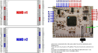
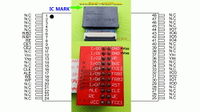
Template:NAND-Flashertable
Jump to navigation
Jump to search
| Chip/PIN | Description | Progskeet | Infectus | 360clip | Description |
|---|---|---|---|---|---|
| NAND 0 | |||||
| 0/1-6 | NC | NC | NC | NC | No Connection |
| 0/7 | R/B | 3 / gp13 | A9 | FRB1 | Read/Busy Output |
| 0/8 | RE | 98 / gp15 | A15 | RE | Read Enable |
| 0/9 | CE | 7 / gp9 | A14 | FCE1 | Chip Enable |
| 0/10+11 | NC | NC | NC | NC | No Connection |
| 0/12 | Vcc | +3.3 | not used / not connected | Vcc | Vcc (min 2.7V-max 3.6V / typ 3.3V) |
| 0/13 | Vss | GND | not used / not connected | GND | VSS - Ground |
| 0/14+15 | NC | NC | NC | NC | No Connection |
| 0/16 | CLE | 4 / gp12 | A13 | CLE | Command Latch Enable |
| 0/17 | ALE | 5 / gp11 | A12 | ALE | Address Latch Enable |
| 0/18 | WE | 2 / gp14 | A11 | WE | Write Enable |
| 0/19 | WP | 6 / gp10 | A10 | WP | Write Protect |
| 0/20-28 | NC | NC | NC | NC | No Connection |
| 0/29 | I/O-0 | 90 / dq8 | A0 | I/O0 | |
| 0/30 | I/O-1 | 91 / dq9 | A1 | I/O1 | |
| 0/31 | I/O-2 | 92 / dq10 | A2 | I/O2 | |
| 0/32 | I/O-3 | 93 / dq11 | A3 | I/O3 | |
| 0/33-35 | NC | NC | NC | NC | No Connection |
| 0/36 | Vss | GND | not used / not connected | GND | VSS - Ground |
| 0/37 | Vcc | +3.3 | not used / not connected | Vcc | Vcc (min 2.7V-max 3.6V / typ 3.3V) |
| 0/38-40 | NC | NC | NC | NC | No Connection |
| 0/41 | I/O-4 | 94 / dq12 | A4 | I/O4 | |
| 0/42 | I/O-5 | 95 / dq13 | A5 | I/O5 | |
| 0/43 | I/O-6 | 96 / dq14 | A6 | I/O6 | |
| 0/44 | I/O-7 | 97 / dq15 | A7 | I/O7 | |
| 0/45-48 | NC | NC | NC | NC | No Connection |
| Chip/PIN | Description | Progskeet | Infectus | Description | |
| NAND 1 | |||||
| 1/1-6 | NC | NC | NC | NC | No Connection |
| 1/7 | R/B | 64 / rdy | U | FRB1 | Read/Busy Output |
| 1/8 | RE | 69 / oe | M | RE | Read Enable |
| 1/9 | CE | 60 / gp3 | N | FCE1 | Chip Enable |
| 1/10+11 | NC | NC | NC | NC | No Connection |
| 1/12 | Vcc | +3.3 | not used / not connected | Vcc | Vcc (min 2.7V-max 3.6V / typ 3.3V) |
| 1/13 | Vss | GND | not used / not connected | GND | VSS - Ground |
| 1/14+15 | NC | NC | NC | NC | No Connection |
| 1/16 | CLE | 63 / gp0 | O | CLE | Command Latch Enable |
| 1/17 | ALE | 62 / gp1 | P | ALE | Address Latch Enable |
| 1/18 | WE | 65 / we | Q | WE | Write Enable |
| 1/19 | WP | 61 / gp2 | T | WP | Write Protect |
| 1/20-28 | NC | NC | NC | NC | No Connection |
| 1/29 | I/O-0 | 79 / dq0 | D0 | I/O0 | |
| 1/30 | I/O-1 | 80 / dq1 | D1 | I/O1 | |
| 1/31 | I/O-2 | 81 / dq2 | D2 | I/O2 | |
| 1/32 | I/O-3 | 82 / dq3 | D3 | I/O3 | |
| 1/33-35 | NC | NC | NC | NC | No Connection |
| 1/36 | Vss | GND | not used / not connected | GND | VSS - Ground |
| 1/37 | Vcc | +3.3 | not used / not connected | Vcc | Vcc (min 2.7V-max 3.6V / typ 3.3V) |
| 1/38-40 | NC | NC | NC | NC | No Connection |
| 1/41 | I/O-4 | 83 / dq4 | D4 | I/O4 | |
| 1/42 | I/O-5 | 84 / dq5 | D5 | I/O5 | |
| 1/43 | I/O-6 | 85 / dq6 | D6 | I/O6 | |
| 1/44 | I/O-7 | 86 / dq7 | D7 | I/O7 | |
| 1/45-48 | NC | NC | NC | NC | No Connection |
| Board trace | |||||
| GND | Vss | not used / not connected | GND | not used / not connected | VSS - Ground |
| +5VDC | Vcc | not used / not connected | 5V | not used / not connected | Vcc from TH3401 (CECHA+CECHB/COK-001) Vcc from TH3401 (CECHC+CECHE/COK-002) Vcc from TH3280 (CECHG/SEM-001) |


