Talk:PS3Cobra Payload Reverse Engineering
D/L's
COBRA v2.0 boot //mirror (TDC) dumpsource
PSGrooPIC Cobra v2.00 (not working)
cobra 2.0 exit from ps2 game+boot of ps2 game at 185632.rar (4.48 MB)
Updater v1.0
http://www.ps3hax.net/2011/10/cobra-v4-1-cobra-usb-ps3-updater-v1-0-released/
- http://www.cobra-usb.com/downloads/Cobra-USB_Firmware_v4.1.rar // Cobra-USB_Manager_v4.1.rar (3.92 MB)
- http://www.cobra-usb.com/downloads/Cobra-USB_Manager_v4.1.rar // Cobra-USB_Firmware_v4.1.rar (174.44 KB)
- http://www.cobra-usb.com/downloads/Cobra-USB_PSP-Launcher.rar // Cobra-USB_PSP-Launcher.rar (332.73 KB)
- http://www.cobra-usb.com/downloads/Cobra-USB_PS3_Updater_v1_0.rar // Cobra-USB_PS3_Updater_v1_0.rar (401.7 KB)
Hardware Dongle
Dongle 1.0
Components
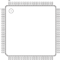
Actel ProASIC3 A3P060 - FPGA
U2
  A3P060 = 60,000 System Gates
  blank = Speed Grade: Standard
  VQ = Package Type: Very Thin Quad Flat Pack (0.5mm pitch)
  G = Lead-Free Packaging: RoHS-Compliant (Green)
  100 = Package Lead Count : 100 pins
  blank = Security Feature : no IP license
  blank = Temperature Range: Commercial (0°C to +70°C Ambient Temperature)
128-bit AES
1,024 bits of user flash memory
Datasheets and usermanuals: http://www.actel.com/products/pa3/docs.aspx#ds
Familyroot: http://www.actel.com/products/pa3/
Pinout A3P060 VQ100
| Pin | Function | Notes |
|---|---|---|
| 1 | GND | Ground |
| 2 | GAA2/IO118UDB3 | |
| 3 | IO118VDB3 | |
| 4 | GAB2/IO117UDB3 | |
| 5 | IO117VDB3 | |
| 6 | GAC2/IO116UDB3 | |
| 7 | IO116VDB3 | |
| 8 | IO112PSB3 | |
| 9 | GND | Ground |
| 10 | GFB1/IO109PDB3 | |
| 11 | GFB0/IO109NDB3 | |
| 12 | VCOMPLF | |
| 13 | GFA0/IO108NPB3 | |
| 14 | VCCPLF | |
| 15 | GFA1/IO108PPB3 | |
| 16 | GFA2/IO107PSB3 | |
| 17 | VCC | |
| 18 | VCCIB3 | |
| 19 | GFC2/IO105PSB3 | |
| 20 | GEC1/IO100PDB3 | |
| 21 | GEC0/IO100NDB3 | |
| 22 | GEA1/IO98PDB3 | |
| 23 | GEA0/IO98NDB3 | |
| 24 | VMV3 | |
| 25 | GNDQ | Ground |
| 26 | GEA2/IO97RSB2 | |
| 27 | GEB2/IO96RSB2 | |
| 28 | GEC2/IO95RSB2 | |
| 29 | IO93RSB2 | |
| 30 | IO92RSB2 | |
| 31 | IO91RSB2 | |
| 32 | IO90RSB2 | |
| 33 | IO88RSB2 | |
| 34 | IO86RSB2 | |
| 35 | IO85RSB2 | |
| 36 | IO84RSB2 | |
| 37 | VCC | |
| 38 | GND | Ground |
| 39 | VCCIB2 | |
| 40 | IO77RSB2 | |
| 41 | IO74RSB2 | |
| 42 | IO71RSB2 | |
| 43 | GDC2/IO63RSB2 | |
| 44 | GDB2/IO62RSB2 | |
| 45 | GDA2/IO61RSB2 | |
| 46 | GNDQ | Ground |
| 47 | TCK | |
| 48 | TDI | |
| 49 | TMS | |
| 50 | VMV2 | |
| 51 | GND | Ground |
| 52 | VPUMP | |
| 53 | NC | |
| 54 | TDO | |
| 55 | TRST | |
| 56 | VJTAG | |
| 57 | GDA1/IO60USB1 | |
| 58 | GDC0/IO58VDB1 | |
| 59 | GDC1/IO58UDB1 | |
| 60 | IO52NDB1 | |
| 61 | GCB2/IO52PDB1 | |
| 62 | GCA1/IO50PDB1 | |
| 63 | GCA0/IO50NDB1 | |
| 64 | GCC0/IO48NDB1 | |
| 65 | GCC1/IO48PDB1 | |
| 66 | VCCIB1 | |
| 67 | GND | Ground |
| 68 | VCC | |
| 69 | IO43NDB1 | |
| 70 | GBC2/IO43PDB1 | |
| 71 | GBB2/IO42PSB1 | |
| 72 | IO41NDB1 | |
| 73 | GBA2/IO41PDB1 | |
| 74 | VMV1 | |
| 75 | GNDQ | Ground |
| 76 | GBA1/IO40RSB0 | |
| 77 | GBA0/IO39RSB0 | |
| 78 | GBB1/IO38RSB0 | |
| 79 | GBB0/IO37RSB0 | |
| 80 | GBC1/IO36RSB0 | |
| 81 | GBC0/IO35RSB0 | |
| 82 | IO29RSB0 | |
| 83 | IO27RSB0 | |
| 84 | IO25RSB0 | |
| 85 | IO23RSB0 | |
| 86 | IO21RSB0 | |
| 87 | VCCIB0 | |
| 88 | GND | Ground |
| 89 | VCC | |
| 90 | IO15RSB0 | |
| 91 | IO13RSB0 | |
| 92 | IO11RSB0 | |
| 93 | GAC1/IO05RSB0 | |
| 94 | GAC0/IO04RSB0 | |
| 95 | GAB1/IO03RSB0 | |
| 96 | GAB0/IO02RSB0 | |
| 97 | GAA1/IO01RSB0 | |
| 98 | GAA0/IO00RSB0 | |
| 99 | GNDQ | Ground |
| 100 | VMV0 |
24.000 MHz Crystal
Y1
CLK for Actel
12.000 MHz Crystal
Y2?
CLK for Atmel
AMS1117 3.3 1032 - Low Dropout Linear Regulator
U3
Datasheet: http://www.sltdigital.com/product/product_pdf/AMS1117.pdf / http://home1.cyber-labo.co.jp/board/goods/pdf/AMS1117.pdf
File:AMS1117 - SOT-223.png
(unreferenced 5pin IC : U4)
U4
51c or s1c ? - hard to see without magnifier
File:SOT5.PNG
Atmel ATmega 16A (16MHz AVR - 16KB flash - USB stack + DFU)
U5
ISP via pin 1 (MOSI), 2 (MISO), 3 (SCK), 4 (Reset)
Winbond 25X16AVS1G (SPI Flash 16Mbit)
U1
W - Winbond
25X - SPI Flash
16 - 16Mbit / 2M-byte (Uniform 4Kbyte sectors/64Kbyte blocks)
AVS1G - 100MHz (200Mbits/sec)
datasheet: W25X16A.pdf (1.3 MB)
Note: can use Bus Ninja or Bus Pirate and FlashROM - ISP is possible, so long as no other devices on the SPI bus are trying to access the device (in that case, you might want to cut Vcc to the FPGA or the regulator for it).
| Pin | Usage | Remarks |
|---|---|---|
| 1 | /CS | Chip Select |
| 2 | DO | Data output |
| 3 | /WP | Write Protect |
| 4 | GND | Ground |
| 5 | DIO | Serial data input/output |
| 6 | CLK | Serial Clock |
| 7 | /HOLD | Hold |
| 8 | VCC | Vcc (min 2.7-max 3.6V) |


