RSX: Difference between revisions
| Line 189: | Line 189: | ||
|} | |} | ||
Other unspecified: CXD297BGB and CXD2971-1GB (CECHA<!--//Pereb//-->) | Other unspecified: CXD297BGB and CXD2971-1GB (CECHA<!--//Pereb//--> refurbished? note:lowest FW was 2.30) | ||
Revision as of 16:48, 10 August 2011
Hardware
RSX - Reality Synthesizer
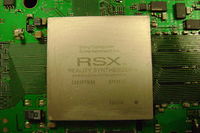
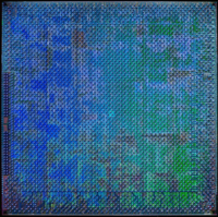
The RSX 'Reality Synthesizer' is a proprietary graphics processing unit (GPU) codeveloped by Nvidia and Sony for the PlayStation 3 game console. It is a GPU based on the Nvidia 7800GTX graphics processor and, according to Nvidia, is a G70/G71 (previously known as NV47) hybrid architecture with some modifications. The RSX has separate vertex and pixel shader pipelines. The GPU makes use of 256 MB GDDR3 RAM clocked at 650 MHz with an effective transmission rate of 1.4 GHz and up to 224 MB of the 3.2 GHz XDR main memory via the CPU (480 MB max).
Specifications
- 500 MHz on 90 nm process (shrunk to 65 nm in 2008 and to 40 nm in 2010)
- Based on NV47 Chip (Nvidia GeForce 7800 Architecture)
- Little Endian
- 300+ million transistors
- Multi-way programmable parallel floating-point shader pipelines
- Independent pixel/vertex shader architecture
- 24 parallel pixel-shader ALU pipes clocked @ 550 MHz
- 5 ALU operations per pipeline, per cycle (2 vector4 , 2 scalar/dual/co-issue and fog ALU, 1 Texture ALU)
- 27 floating-point operations per pipeline, per cycle
- 8 parallel vertex pipelines
- 2 ALU operations per pipeline, per cycle (1 vector4 and 1 scalar, dual issue)
- 10 FLOPS per pipeline, per cycle
- Floating Point Operations: 400.4 Gigaflops ((24 * 27 Flops + 8 * 10 Flops) * 550)
- 24 texture filtering units (TF) and 8 vertex texture addressing units (TA)
- 24 filtered samples per clock
- Maximum Texel fillrate: 12.0 GigaTexels per second (24 textures * 500 MHz)
- 32 unfiltered texture samples per clock, ( 8 TA x 4 texture samples )
- 24 filtered samples per clock
- 8 Render Output units / pixel rendering pipelines
- Peak pixel fillrate (theoretical): 4.0 Gigapixel per second
- Maximum Z-buffering sample rate: 8.0 GigaSamples per second (2 Z-samples * 8 ROPs * 500 MHz)
- Maximum Dot product operations: 51 billion per second (combined with Cell CPU)
- 128-bit pixel precision offers rendering of scenes with High dynamic range rendering
- 256 MB GDDR3 RAM at 650 MHz
- Earlier PS3 Models: Samsung K4J52324QC-SC14 rated at 700Mhz
- Later PS3 Models: Qimonda HYB18H512322AF-14
- 128-bit memory bus width
- 22.4 GB/s read and write bandwidth
- Cell FlexIO bus interface
- Rambus XDR Memory interface bus width: 56bit out of 64bit (serial)
- 20 GB/s read to the Cell and XDR memory
- 15 GB/s write to the Cell and XDR memory
- Support for PSGL (OpenGL ES 1.1 + Nvidia Cg)
- Support for S3 Texture Compression
More features are revealed in the following chart delineating the differences between the RSX and the nVidia 7800 GTX.
| Difference | RSX | nVidia 7800GTX |
|---|---|---|
| GDDR3 Memory bus | 128bit | 256bit |
| ROPs | 8 | 16 |
| Post Transform and Lighting Cache | 63 max vertices | 45 max vertices |
| Total Texture Cache Per Quad of Pixel Pipes (L1 and L2) | 96kB | 48kB |
| CPU interface | FlexIO | PCI-Express 16x |
| Technology | 40nm/65nm/90nm | 110nm |
Other RSX features/differences include:
   More shader instructions
       Extra texture lookup logic (helps RSX transport data from XDR)
       Fast vector normalize
Note that the cache (Post Transform and Lighting Vertext Cache) is located between the vector shader and the triangle setup.
A sample flow of data inside the RSX would see them first processed by 8 vertex shaders. The output are then sent to the 24 active pixel shaders, which can involve the 24 active texture units. Finally, the data is passed to the 8 Raster Operation Pipeline units (ROPs), and on out to the GDDR3. Note that the pixel shaders are grouped into groups of four (called Quads). There are 7 Quads, with 1 redundant, leaving 6 Quads active, which provides us with the 24 active pixel shaders listed above (6 times 4 equals 24). Since each Quad has 96kB of L1 and L2 cache, the total RSX texture cache is 576kB. General RSX features include 2x and 4x hardware anti-aliasing, and support for Shader Model 3.0.
RSX Memorymap
Although the RSX has 256MB of GDDR3 RAM, not all of it is useable. The last 4MB is reserved for keeping track of the RSX internal state and issued commands. The 4MB of GPU Data contains RAMIN, RAMHT, RAMFC, DMA Objects, Graphic Objects, and the Graphic Context. The following is a breakdown of the address within 256MB of the RSX.
| Address Range | Size | Comment |
|---|---|---|
| 0000000-FBFFFFF | 252 MB | Framebuffer |
| FC00000-FFFFFFF | 4 MB | GPU Data |
| FF80000-FFFFFFF | 512KB | RAMIN: Instance Memory |
| FF90000-FF93FFF | 16KB | RAMHT: Hash Table |
| FFA0000-FFA0FFF | 4KB/s | RAMFC: FIFO Context |
| FFC0000-FFCFFFF | 64KB | DMA Objects |
| FFD0000-FFDFFFF | 64KB | Graphic Objects |
| FFE0000-FFFFFFF | 128KB | GRAPH: Graphic Context |
Chipnumers @ SKU's
The following is a small sample of serial numbers of the RSX by model number.
| PS3 Model | Mobo serial | RSX Serial | Die Tech | Die Size | Remark |
|---|---|---|---|---|---|
| CECHA | - | CXD2971GB | 90nm | 258mm² | edepot ps3secrets |
| CECHA | 1-871-868-12 | CXD2971AGB | 90nm | 258mm² | reballing.es |
| CECHA | 1-871-868-22 | CXD2971DGB | 90nm | 258mm² | reballing.es |
| CECHA | 1-871-868-32 | CXD2971DGB | 90nm | 258mm² | reballing.es |
| CECHA | 1-871-868-32 | CXD2971AGB | 90nm | 258mm² | reballing.es |
| CECHB | 1-871-868-22 | CXD2971DGB | 90nm | 258mm² | edepot ps3secrets |
| CECHB | 1-871-868-32 | CXD2971DGB | 90nm | 258mm² | edepot ps3secrets |
| CECHC | - | CXD2971DGB | 90nm | 258mm² | edepot ps3secrets |
| CECHC | 1-873-513-21 | CXD2971GB | 90nm | 258mm² | reballing.es |
| CECHC | 1-873-513-31 | CXD2971DGB | 90nm | 258mm² | reballing.es |
| CECHD | unreleased | - | 90nm | 258mm² | - |
| CECHE | -? | -? | 90nm | 258mm² | - |
| CECHF | unreleased | - | 90nm | 258mm² | - |
| CECHG | 1-875-384-11 | CXD2971DGB | 90nm | 258mm² | reballing.es |
| CECHG | 1-875-384-31 | CXD2971DGB | 90nm | 258mm² | reballing.es |
| CECHG | 1-875-384-21 | CXD2971AGB | 90nm | 258mm² | reballing.es |
| CECHG | - | CXD2971DGB | 90nm | 258mm² | edepot ps3secrets |
| CECHH | 1-875-938-11 | CXD2971AGB | 90nm | 258mm² | reballing.es |
| CECHH | 1-875-938-31 | CXD2971-1GB | 90nm | 258mm² | reballing.es |
| CECHH | 1-875-938-31 | CXD2971AGB | 90nm | 258mm² | reballing.es |
| CECHH | - | CXD2971AGB | 90nm | 258mm² | edepot ps3secrets |
| CECHI | unreleased | - | 90nm | 258mm² | - |
| CECHJ | -? | -? | 65nm | ? 186mm² ? | - |
| CECHK | 1-876-912-42 | CXD2982GB | 65nm | ? 186mm² ? | reballing.es |
| CECHK | - | CXD2982GB | 65nm | ? 186mm² ? | edepot ps3secrets |
| CECHL | 1-878-196-31 | CXD2991GB | 65nm | ? 186mm² ? | reballing.es |
| CECHL | - | CXD2991GB | 65nm | ? 186mm² ? | edepot ps3secrets |
| CECHM | -? | -? | 65nm | ? 186mm² ? | - |
| CECHN | unreleased | - | 65nm | ? 186mm² ? | - |
| CECHO | unreleased | - | 65nm | ? 186mm² ? | - |
| CECHP | -? | -? | 65nm | ? 186mm² ? | - |
| CECHQ | -? | -? | 65nm | ? 186mm² ? | - |
| CECH-2001A | - | CXD2991CGB | 65nm | ? 186mm² ? | reballing.es |
| CECH-2001B | 1-880-055-31 | CXD2991EGB | 65nm | ? 186mm² ? | reballing.es |
| CECH-20xx | - | CXD2991EGB | 65nm | ? 186mm² ? | edepot ps3secrets |
| CECH-2101A | 1-881-945-11 | CXD5300AGB | 40nm | ? 114mm² ? | reballing.es |
| CECH-21xx | - | CXD5300AGB | 40nm | ? 114mm² ? | edepot ps3secrets |
| CECH-25xx | - | CXD5300A1GB | 40nm | ? 114mm² ? | edepot ps3secrets |
| CECH-30xx | -? | CXD5301DGB | 40nm? | 114mm²? | - |
Other unspecified: CXD297BGB and CXD2971-1GB (CECHA refurbished? note:lowest FW was 2.30)
Alternative list:
- CECHA/COK-001, CECHB/COK-001, CECHC/COK-002 and CECHH/DIA-001 : CXD2971AGB (RSX 90nm)
- CECHG/SEM-001 : CXD2971DGB (RSX 90nm)
- CECHJ/DIA-002 and CECHK/DIA-002 : CXD2982 (RSX 65nm)
- CECHL/VER-001 up to including CECHQ/VER-001 : CXD2991BGB (RSX 65nm)
- CECH-20../DYN-001 : CXD2991GGB (RSX 65nm)
- CECH-21../SUR-001 : CXD5300AGB (RSX 40nm)
- CECH-250./JTP-001 : CXD5300A1GB (RSX 40nm)
- CECH-30../KTE-001 : CXD5301DGB (RSX 40nm)
Speed, Bandwidth, and Latency
System bandwith (theoretical maximum):
- Cell to/from 256MB XDR : 25.6 GB/s
- Cell to RSX (IOIFO): 20GB/s (practical : 15.8GB/s @ packetsize 128B)
- Cell from RSX (IOIFI) : 15GB/s (practical : 11.9GB/s @ packetsize 128B)
- RSX to/from 256MB GDDR3 : 20.8GB/s (@ 650MHz)
Because of the aforementioned layout of the communication path between the different chips, and the latency and bandwidth differences between the various components, there are different access speeds depending on the direction of the access in relation to the source and destination. The following is a chart showing the speed of reads and writes to the GDDR3 and XDR memory from the viewpoint of the Cell and RSX. Note that these are measured speeds (rather than calculated speeds) and they should be worse if RSX and GDDR3 access are involved because these figures were measured when the RSX was clocked at 550Mhz and the GDDR3 memory was clocked at 700Mhz. The shipped PS3 has the RSX clocked in at 500Mhz (front and back end, although the pixel shaders run separately inside at 550Mhz). In addition, the GDDR3 memory was also clocked lower at 650Mhz.
| Processor | 256MB XDR | 256MB GDDR3 |
|---|---|---|
| Cell Read | 16.8GB/s | 16MB/s (15.6MB/s @ 650MHz) |
| Cell Write | 24.9GB/s | 4GB/s |
| RSX Read | 15.5GB/s | 22.4GB/s (20.8GB/s @ 650MHz) |
| RSX Write | 10.6GB/s | 22.4GB/s (20.8GB/s @ 650MHz) |
Because of the VERY slow Cell Read speed from the 256MB GDDR3 memory, it is more efficient for the Cell to work in XDR and then have the RSX pull data from XDR and write to GDDR3 for output to the HDMI display. This is why extra texture lookup instructions were included in the RSX to allow loading data from XDR memory (as opposed to the local GDDR3 memory).
RSX Libraries
The RSX is dedicated to 3D graphics, and developers are able to use different API libraries to access its features. The easiest way is to use high level PSGL, which is basicially OpenGL|ES with programmable pipeline added in - but hardly anyone uses PSGL these days, preferring to use the native GPU command buffer generation library, libgcm. At a lower level developers can use LibGCM, which is an API that talks to the RSX at a lower level. PSGL is actually implemented on top of LibGCM. For the advanced programmer, you can program the RSX by sending commands to it directly using C or assembly. This can be done by setting up commands (via FIFO Context) and DMA Objects and issuing them to the RSX via DMA calls.
Pad/pinouts
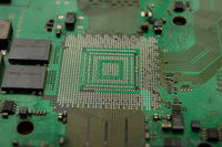
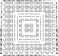
Padout IC2001 (RSX)
Productcode: CXD2971GB | PartNo.: 8-753-251-46
FC-BGA: 41x41 (1681) with empty center patterned 19x19 (-?) = ? when not counting missing/not used pads
package size: 42.5mm x 42.5mm | pad pitch: 1.00mm                <-- need confirmation
package material: ? (if ceramic: FC-CBGA, if plastic: FC-PBGA)   <-- need confirmation
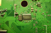
Pinout IC2101 (2 channel Thermal Monitor SMbus IC)
OnSemi ADT7461A0002RMZR
6-710-286-01 / IC2101
Datasheet: ADT7461-D.PDF
http://www.ps3devwiki.com/index.php?title=File:ADT7461A0002RMZR.png
Used for monitoring the RSX
| Pin | Signal | Description |
|---|---|---|
| 1 | VCC | +3.3_Thermal |
| 2 | D+ | from RSX_TDR via R2101 100 Ohm and C2103 0.001uF 50V |
| 3 | D- | from RSX_TDN via R2102 100 Ohm and C2103 0.001uF 50V |
| 4 | /THERM | to RSX_GPIO6 / RSX_THR_EVENT |
| 5 | GND | Ground |
| 6 | /THERM2 | to /THRRSX_SENS_ALRT |
| 7 | SDATA | from THR_I2C_SDA |
| 8 | SCLK | from THR_I2C_SCL |
Pinout IC2102
ICS ICS422AG-07LFT
6-710-158-01 / IC2102
http://www.ps3devwiki.com/index.php?title=File:ICS_422AG07LF.JPG
Used for RSX AV_CLK
| Pin | Signal | Description |
|---|---|---|
| 1 | XIN | from X2101 24.576MHz |
| 2 | VDD | +3.3V_ANA via FB2101 0 uH |
| 3 | GND | Ground |
| 4 | 54M | to RSX_AVCLK0 via R2103 43.2 Ohm |
| 5 | GND | Ground |
| 6 | VDD54 | +1.5_AVCG_VDDIO via FB2102 0 uH |
| 7 | VDD | +3.3V_ANA via FB2101 0 uH |
| 8 | GND | Ground |
| 9 | 53.946M | to RSX_AVCLK1 via R2104 43.2 Ohm |
| 10 | GND | Ground |
| 11 | VDD53 | +1.5_AVCG_VDDIO via FB2102 0 uH |
| 12 | OE | from SW_AVCG |
| 13 | SEL | from RSX_GPIO0 |
| 14 | VDDAUD | +1.5_AVCG_VDDIO via FB2102 0 uH |
| 15 | GND | Ground |
| 16 | AUDIO | to pin2 IC2105 via R2117 / to RSX_AVCLK3 via R2109 39 Ohm |
| 17 | GND | Ground |
| 18 | VDD | +3.3V_ANA via FB2101 0 uH |
| 19 | VDD | +3.3V_ANA via FB2101 0 uH |
| 20 | GND | Ground |
| 21 | 24.576M | to RSX_AVCLK2 via R2108 43.2 Ohm |
| 22 | GND | Ground |
| 23 | VDDREF | +1.5_AVCG_VDDIO via FB2102 0 uH |
| 24 | XOUT | to X2101 24.576MHz via R2107 0 Ohm |
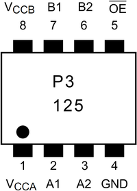
Pinout IC2105 (2bit Dual Supply Bus Buffer)
Toshiba TC7WP3125FK(T5RSOF
6-710-429-01 / IC2105, IC2501
Datasheet: TC7WP3125FC_TC7WP3125FK_en_datasheet_080602.pdf
http://www.ps3devwiki.com/index.php?title=File:TC7WP3125FK.png
Used for RSX Audio
| Pin | Signal | Description |
|---|---|---|
| 1 | VCCA | +1.5V_AVCG_VDDIO |
| 2 | A1 | from pin16 (audio) of IC2102 (ICS ICS422AG-07LFT) via R2117 43.2 Ohm |
| 3 | A2 | to Ground |
| 4 | GND | Ground |
| 5 | /OE | to PCLKEN via buffer Q2101 (DTC144EUA-T106) / R2180 10K Ohm |
| 6 | B2 | - |
| 7 | B1 | to DRCG_GEN18M via R2123 33 Ohm |
| 8 | VCCB | from 1.8V_EEGS_VDDIO via R2122 0 Ohm |
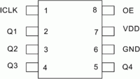
Pinout IC2108 (Low Skew 1 To 4 Clock Buffer)
ICS ICS651MLFT
6-710-430-01 / IC2108
Datasheet: ICS651MLFT.pdf (185.76 KB)
http://www.ps3devwiki.com/index.php?title=File:ICS651MLFT-SOIC8P.png
Used for RSX Audio
| Pin | Signal | Description |
|---|---|---|
| 1 | ICLK | from RS_MCLKO0 |
| 2 | Q1 | to HDMI_MCLKO0 via R2177 33 Ohm |
| 3 | Q2 | - |
| 4 | Q3 | to ADAC_MCLKO0 via R2179 33 Ohm |
| 5 | Q4 | - |
| 6 | GND | Ground |
| 7 | VDD | +1.5V_RSX_VDDIO |
| 8 | OE | to +1.5V_RSX_VDDIO |
Drivers (WiP/reference)
Other References
http://7track.org/~durandal/ps3dox/http://lol.notsoldierx.com/~durandal/ps3dox/ // http://173.220.0.157/~durandal/ps3dox/- http://wiki.ps2dev.org/ps3:rsx
- Cg Toolkit User's Manual: A Developer's Guide to Programmable Graphics, Release 1.4.1
- The Cg Tutorial (ISBN: 0321194969, Addison-Wesley, 2003)
- cg-shader-tutorial.pdf (535.94 KB) + Git: Emulator-Shader-Pack
