File:PS3 DualNand Retail ProgSkeet.png
Jump to navigation
Jump to search
Size of this preview: 800 × 432 pixels. Other resolution: 1,192 × 644 pixels.
Original file (1,192 × 644 pixels, file size: 711 KB, MIME type: image/png)
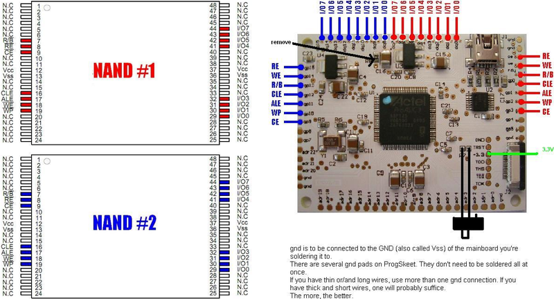
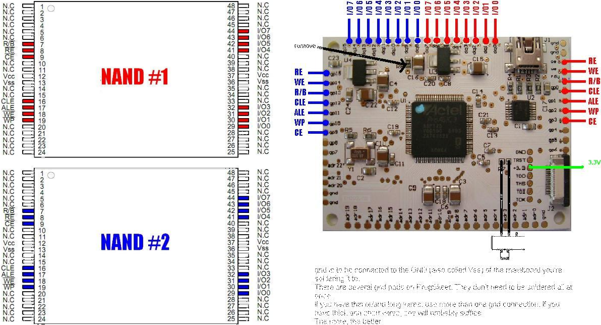
Dual NAND connection to Progskeet diagram
Text below PCB pic:
gnd is to be connected to the GND (also called Vss) of the mainboard you´re soldering it to.
There are gnd pads on ProgSkeet. They don´t need to be soldered all at once.
If you have thin/or/and long wires, use more than one gnd connection.
If you have thick and short wires, one will probably suffice.
The more, the better...
File history
Click on a date/time to view the file as it appeared at that time.
| Date/Time | Thumbnail | Dimensions | User | Comment | |
|---|---|---|---|---|---|
| current | 19:49, 3 August 2011 | | 1,192 × 644 (711 KB) | Euss (talk | contribs) | Category:HardwareDual NAND connection to Progskeet diagram |
You cannot overwrite this file.
File usage
The following 3 pages use this file: