Graphics Synthesizer: Difference between revisions
Jump to navigation
Jump to search
m (Added CXD2949CGB confirmed on GH-032 motherboard.) |
mNo edit summary |
||
| Line 10: | Line 10: | ||
** 279 mm² die size | ** 279 mm² die size | ||
** Announced at ISSCC 99, not used in any final/consumer consoles | ** Announced at ISSCC 99, not used in any final/consumer consoles | ||
* 0. | * 0.08: CXD2934GB | ||
** 188 mm² die size | ** 188 mm² die size | ||
** 19 W power consumption | ** 19 W power consumption | ||
| Line 17: | Line 17: | ||
** Used on [[motherboards]]: GH-001, GH-003, GH-005, GH-007, GH-012, GH-014, GH-016 | ** Used on [[motherboards]]: GH-001, GH-003, GH-005, GH-007, GH-012, GH-014, GH-016 | ||
** [[File:Ps9pRpU.jpg|200px]] | ** [[File:Ps9pRpU.jpg|200px]] | ||
* 1. | * 1.05: CXD2944GB | ||
** 180nm process node, 108 mm² die size | ** 180nm process node, 108 mm² die size | ||
** plastic case, very different pinout | ** plastic case, very different pinout | ||
** Copyright date: 2000 | ** Copyright date: 2000 | ||
** Used on motherboards: GH-004, GH-006, GH-008, GH-010, GH-013 | ** Used on motherboards: GH-004, GH-006, GH-008, GH-010, GH-013 | ||
* 1. | * 1.09: CXD2949GB (reported as CXD2949BGB in PS2ident) | ||
** 96 mm² die size (?) | ** 96 mm² die size (?) | ||
** different pinout, no analog RGB output (now generated by external DAC) | ** different pinout, no analog RGB output (now generated by external DAC) | ||
** Copyright date: 2001 | ** Copyright date: 2001 | ||
** Used on motherboards: GH-015, GH-017 - GH-023 (except GH-016) | ** Used on motherboards: GH-015, GH-017 - GH-023 (except GH-016) | ||
* 1. | * 1.09: CXD2949BGB | ||
** 96 mm² die size (?) | ** 96 mm² die size (?) | ||
** Copyright date: 2001 | ** Copyright date: 2001 | ||
Revision as of 03:46, 12 August 2024
Overview
"GS" stands for Graphics Synthesizer. It's the PlayStation®2's co-processor that's responsible for rendering the graphics (but is also used by some games for additional calculations and other purposes). It runs at half of the Emotion Engine's Clock speed at 147.456 MHz.
The first revision released, CXD2934GB, is known to have been manufactured using a 180 nm process and to consume 19 W of power (calculated from the official information that the initially released Emotion Engine consumed 18 W of power and that EE and GS together initially consumed 37 W of power).
There have been die-shrinks and optimizations over the years.
Revisions
- Press Release
- 279 mm² die size
- Announced at ISSCC 99, not used in any final/consumer consoles
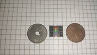
- 0.08: CXD2934GB
- 188 mm² die size
- 19 W power consumption
- metal IHS
- Copyright date: 1999
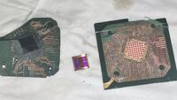
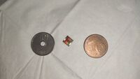
- Used on motherboards: GH-001, GH-003, GH-005, GH-007, GH-012, GH-014, GH-016
- 1.05: CXD2944GB
- 180nm process node, 108 mm² die size
- plastic case, very different pinout
- Copyright date: 2000
- Used on motherboards: GH-004, GH-006, GH-008, GH-010, GH-013
- 1.09: CXD2949GB (reported as CXD2949BGB in PS2ident)
- 96 mm² die size (?)
- different pinout, no analog RGB output (now generated by external DAC)
- Copyright date: 2001
- Used on motherboards: GH-015, GH-017 - GH-023 (except GH-016)
- 1.09: CXD2949BGB
- 96 mm² die size (?)
- Copyright date: 2001
- Used on motherboards: GH-015, GH-017 - GH-023 (except GH-016)
- 1.11: CXD2949CGB
- 83 mm² die size (?)
- Copyright date: 2002
- Used on motherboards: GH-023 - GH-032 (Confirmed use on GH-032 boards?)
- 1.11: CXD2949DGB
- 73 mm² die size (?)
- Copyright date: 2003
- Used on motherboards: ? - GH-032-54 - GH-041
- CXD2972GB
- 49 mm² die size
- likely 90 nm process
- Copyright date: 2006
- Used on motherboards: PlayStation 3 with COK-002/COK-002W (CECHC and CECHE models)
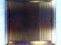
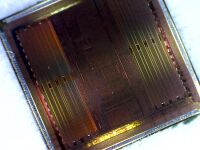
- Dieshots confirming that this is indeed just a GS and not an EE+GS variant (unlike EE+GS in CECHA and CECHB PS3 consoles)
- 1.1?: CXD2980GB
- Differences to the other CXD2980xGB revisions are unknown
- GS was made a separate IC again after combining EE with RDRAM, IOP and other components instead
- Copyright date: 2007
- Used on motherboards: GH-061-22 (likely others as well; please contribute)
- 1.14: CXD2980AGB (sometimes reported as CXD2980CGB in PS2ident)
- Differences to the other CXD2980xGB revisions are unknown
- GS was made a separate IC again after combining EE with RDRAM, IOP and other components instead
- Copyright date: 2007
- Used on motherboards: GH-061-12 (likely others as well; please contribute)
- 1.14: CXD2980CGB
- Differences to the other CXD2980xGB revisions are unknown
- GS was made a separate IC again after combining EE with RDRAM, IOP and other components instead
- Has no cooling at all besides airflow
- Copyright date: 2007
- Used on motherboards: GH-061-51, GH-070-42 (likely others as well; please contribute)
- 1.15: CXD2980BGB
- Differences to the other CXD2980xGB revisions are unknown
- Has no cooling at all besides airflow
- 49 mm² die size (identical to CXD2972GB found on PS3's COK-002, despite the BGA case being much smaller)
- likely 90 nm process
- Used on motherboards: GH-061-12 - GH-072-42, can thus be used in every 790xx and 900xx slim PS2
- Copyright date: 2007
Specifications
- Parallel rendering processor with embedded DRAM "Graphics Synthesizer" (GS) clocked at 147.456 MHz
- Programmable CRT controller (PCRTC) for output
- Pixel pipelines: 16 without any texture mapping units (TMU), however half of pixel pipelines can perform texturing, so fillrate is either 16 pixels per clock with untextured 2400 Mpixels; or 8 pixels per clock with 1200 megapixels with bilinear texturing, and 1200 megatexels (bilinear).
- Video output resolution: Variable from 256×224 to 1920×1080
- 4 MB of embedded DRAM as video memory (an additional 32 MB of main memory can be used as video memory); 48 gigabytes per second peak bandwidth
- Texture buffer bandwidth: 9.6 GB/s
- Frame buffer bandwidth: 38.4 GB/s
- eDRAM bus width: 2560-bit (composed of three independent buses: 1024-bit write, 1024-bit read, 512-bit read/write)
- Pixel configuration: RGB:alpha, 24:8, 15:1; 16-, 24-, or 32-bit Z-buffer
- Display color depth: 32-bit (RGBA: 8 bits each)
- Dedicated connection to main CPU and VU1
- Overall pixel fillrate: 16 × 147 Mpix/s = 2.352 gigapixel/s
- 1.2 gigapixel/s (with Z-buffer, alpha, and texture)
- With no texture, flat shaded: 2.4 Gpix/s (75,000,000 32-pixel raster triangles)
- With 1 full texture (diffuse map), Gouraud shaded: 1.2 Gpix/s (37,750,000 32-bit pixel raster triangles)
- With 2 full textures (diffuse map and specular, alpha, or other), Gouraud shaded: 0.6 Gpix/s (18,750,000 32-bit pixel raster triangles)
- Texture fillrate: 1.2 Gtexel/s
- Sprite drawing rate: 18.75 million/s (8×8 pixels)
- Particle drawing rate: 150 million/s
- Polygon drawing rate: 75 million/s (small polygon)
- 50 million/s (48-pixel quad with Z and A)
- 30 million/s (50-pixel triangle with Z and A)
- 25 million/s (48-pixel quad with Z, A and T)
- 16 million/s (75-pixel triangle with Z, A, T and fog)
- VESA (maximum 1280×1024 pixels)
- 3 rendering paths (path 1, 2 and 3) GS effects include: Dot3 bump mapping (normal mapping), mipmapping, spherical harmonic lighting, alpha blending, alpha test, destination alpha test, depth test, scissor test, transparency effects, framebuffer effects, post-processing effects, perspective-correct texture mapping, edge-AAx2 (poly sorting required), bilinear, trilinear texture filtering, multi-pass, palletizing (6:1 ratio 4-bit; 3:1 ratio 8-bit), offscreen drawing, framebuffer mask, flat shading, Gouraud shading, cel shading, dithering, texture swizzling.
- Multi-pass rendering ability
- Four passes: 300 Mpixel/s (300 Mpixels/s divided by 32 pixels = 9,375,000 triangles/s lost every four passes)
