CPU
Jump to navigation
Jump to search
Overview
LSI CoreWare CW33300-based core
- MIPS R3000A-compatible 32-bit RISC CPU MIPS R3051 with 5 KB L1 cache, running at 33.8688 MHz
- The microprocessor was manufactured by LSI Logic Corp. with technology licensed from SGI
- Features:
- Initial feature size (process node) was 0.5 micron (500 nm)
- 850k – 1M transistors
- Operating performance: 30 MIPS
- Bus bandwidth 132 MB/s
- One arithmetic/logic unit (ALU)
- One shifter
- CPU cache:
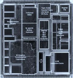
- 4 KB instruction cache
- 1 KB non-associative SRAM data cache
Geometry Transformation Engine (GTE)
- Coprocessor that resides inside the main CPU processor, giving it additional vector math instructions used for 3D graphics, lighting, geometry, polygon and coordinate transformations - GTE performs high-speed matrix multiplications
- Operating performance: 66 MIPS
- Polygons per second (rendered in hardware):
- 90,000 with texture mapping, lighting and Gouraud shading
- 180,000 with texture mapping
- 360,000 with flat shading
Motion Decoder (MDEC)
- Also residing within the main CPU, enables full screen, high quality FMV playback and is responsible for decompressing images and video into VRAM
- Operating performance: 80 MIPS
- Documented device mode is to read three RLE-encoded 16×16 macroblocks, run IDCT and assemble a single 16×16 RGB macroblock
- Output data may be transferred directly to GPU via DMA
- It is possible to overwrite IDCT matrix and some additional parameters, however MDEC internal instruction set was never documented
- It is directly connected to a CPU bus
System Control Coprocessor (Cop0)
- This unit is part of the CPU. Has 16 32-bit control registers
- Modified from the original R3000A cop0 architecture, with the addition of a few registers and functions
- Controls memory management through virtual memory technique, system interrupts, exception handling, and breakpoints
Revisions
CXD8530
- CXD8530Q
- Found on some PU-7, very early/launch units
- Die size: 128 mm², 1M transistors
- Manufactured in 0.6 µm
- Comes in a metal QFP package
- CXD8530AQ
- Found on some PU-7, mostly early/launch units
- Die size: 128 mm², 1M transistors
- Comes in a metal QFP package
- CXD8530BQ
- Found on some PU-7
- Die size: 66 mm²
- This revision and all later revisions are implemented in standard cells as an ASIC, which means there are less visible structures on the die
- This revision and all later revisions come in a plastic QFP package
- CXD8530CQ
- Found on some PU-8 and PU-16
- Die size: 66 mm²
CXD8606
From PU-18 onwards (SCPH-55XX), only CXD8606 was used.
- CXD8606Q
- Found on some PU-8 and PU-18
- Die size: 66 mm², 850k transistors
- Manufactured in 350 nm
- CXD8606AQ
- Found on some PU-18
- Die size: 26.5 mm²
- CXD8606BQ
- Found on some PU-20 as well as PU-22, PU-23 and earlier PM-41
- Die size: 26.5 mm²
- Identical die size to CXD8606AQ
- CXD8606CQ
- Found on later PM-41
CXD8661
- CXD8661R
- Used in some arcade systems (Capcom ZN-2, Namco System 12)
- Runs at considerably higher clock speeds
Pictures
Comparison
[[File:PS1 die sizes.jpg|left|thumb|alt=Properly scaled comparison of die shots of most PS1 CPU revisions. Created by @Siliconinsid (Siliconinsider)|Properly scaled comparison of die shots of most PS1 CPU revisions. Created by [https://twitter.com/Siliconinsid/ @Siliconinsid (Siliconinsider)
Single dice
Relative size of these pictures is not to scale. See above for actual sizes.
 |
 |
 |

|
| Dieshot of CXD8530Q taken from Ken Kutaragis presentation at Hot Chips '99. |
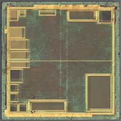
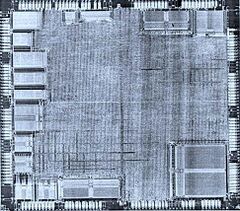
Dieshot of CXD8530CQ taken from zeptobars.com. | Dieshot of CXD8606Q taken from Ken Kutaragis presentation at Hot Chips '99. |
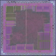
Dieshot of CXD8606BQ by TICS/onidev |