Samsung K8Q2815UQB-PI4B (NOR)[edit | edit source]

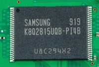
Samsung K8Q2815UQB-PI4B (NOR) as seen on modern PS3 Slim

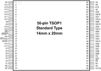
56-pin TSOP1 Standard Type
14mm x 20mm
mirror
mirror
productcode meaning:
K - Memory
8 - NOR Flash
Q - Small Classification : Page Mode DDP
28 - Density : 128M, 8M / 16Bank / 8^8
15 - Dual Bank Boot Block (Bank1, Bank2) : 16M, 2M / 14M
U - Vcc : 3.0V / 3.3V (2.7V~3.6V)
Q - Device Type: Top and Bottom Boot Block
B - Generation : 3rd Generation
-
P - Package : TSOP1 (Lead Free)
I - Temp : Industrial
4B - Speed : 60ns/25ns (Page)
NOTE
Multiple Bank architectures (8 banks)
- Bank 0 :  8Mbit (4Kw x 8 and 32Kw x 15)
- Bank 1 : 24Mbit (32Kw x 48)
- Bank 2 : 24Mbit (32Kw x 48)
- Bank 3 :  8Mbit (4Kw x 8 and 32Kw x 15)
- Bank 4 :  8Mbit (4Kw x 8 and 32Kw x 15)
- Bank 5 : 24Mbit (32Kw x 48)
- Bank 6 : 24Mbit (32Kw x 48)
- Bank 7 :  8Mbit (4Kw x 8 and 32Kw x 15)
OTP Block : Extra 256 word
- 128word for factory and 128word for customer OTP (only on first Virtual Chip, A22=low)
| Pin |
Usage |
Remarks
|
| 1 |
NC |
No Connection
|
| 2 |
A22 |
Virtual Chip Enable of 2nd Chip
|
| 3 |
A15 |
|
| 4 |
A14 |
|
| 5 |
A13 |
|
| 6 |
A12 |
|
| 7 |
A11 |
|
| 8 |
A10 |
|
| 9 |
A9 |
|
| 10 |
A8 |
|
| 11 |
A19 |
|
| 12 |
A20 |
|
| 13 |
WE |
Write Enable
|
| 14 |
RESET |
Reset
|
| 15 |
A21 |
|
| 16 |
WP/ACC |
Write Protect / Accelerated Program Operation
|
| 17 |
RD/BY |
Ready/Busy Output
|
| 18 |
A18 |
|
| 19 |
A17 |
|
| 20 |
A7 |
|
| 21 |
A6 |
|
| 22 |
A5 |
|
| 23 |
A4 |
|
| 24 |
A3 |
|
| 25 |
A2 |
|
| 26 |
A1 |
|
| 27 |
NC |
No Connection
|
| 28 |
NC |
No Connection
|
| Pin |
Usage |
Remarks
|
| 29 |
VCCQ |
VccQ
|
| 30 |
NC |
No Connection
|
| 31 |
A0 |
|
| 32 |
CE |
Chip Enable
|
| 33 |
VSS |
Ground
|
| 34 |
OE |
Output Enable
|
| 35 |
DQ0 |
|
| 36 |
DQ8 |
|
| 37 |
DQ1 |
|
| 38 |
DQ9 |
|
| 39 |
DQ2 |
|
| 40 |
DQ10 |
|
| 41 |
DQ3 |
|
| 42 |
DQ11 |
|
| 43 |
Vcc |
Vcc (min 2.7V-max 3.6V / typ 3.0V)
|
| 44 |
DQ4 |
|
| 45 |
DQ12 |
|
| 46 |
DQ5 |
|
| 47 |
DQ13 |
|
| 48 |
DQ6 |
*OTP?
|
| 49 |
DQ14 |
|
| 50 |
DQ7 |
*OTP?
|
| 51 |
DQ15 |
|
| 52 |
VSS |
Ground
|
| 53 |
NC |
No Connection
|
| 54 |
A16 |
|
| 55 |
NC |
No Connection
|
| 56 |
NC |
No Connection
|
- OTP Block Region : 256-word Flash memory region. The data DQ6=1 for customer locked and DQ7=1 for factory locked
Offset(h) 00 01 02 03 04 05 06 07 08 09 0A 0B 0C 0D 0E 0F
00000000  51 52 59 02 00 40 00 00 00 00 00 27 36 00 00 03  QRY..@.....'6...
00000010  00 09 00 04 00 04 00 17 01 00 00 00 03 07 00 20  ...............
00000020  00 7D 00 00 01 07 00 20 00 00 00 00 00 00 00 00  .}..... ........
00000030  50 52 49 30 30 00 02 01 01 01 01 00 02 85 95 04  PRI00........…•.
00000040  00 00 00 00 00 00 00 00 00 00 00 00 00 00 00 00  ................
00000050  00 00 00 00 00 00 00 00 00 00 00 00 00 00 00 00  ................
00000060  00 00 00 00 00 00 00 00 00 00 00 00 00 00 00 00  ................
00000070  00 00 00 00 00 00 00 00 00 00 00 00 00 00 00 00  ................
00000080  00 00 00 00 00 00 00 00 00 00 00 00 00 00 00 00  ................
00000090  00 00 00 00 00 00 00 00 00 00 00 00 00 00 00 00  ................
000000A0  00 00 00 00 00 00 00 00 00 00 00 00 00 00 00 00  ................
000000B0  00 00 00 00 00 00 00 00 00 00 00 00 00 00 00 00  ................
000000C0  00 00 00 00 00 00 00 00 00 00 00 00 00 00 00 00  ................
000000D0  00 00 00 00 00 00 00 00 00 00 00 00 00 00 00 00  ................
000000E0  00 00 00 00 00 00 00 00 00 00 00 00 00 00 00 00  ................
000000F0  00 00 00 00 00 00 00 00 00 00 00 00 00 00 00 00  ................
